nrf54L15 PCB Design Review for IoT Device

I have been working on a soil moisture sensor for my indoor plants and I wanted to build some skills in PCB design using a Nordic SoC. I have chosen the nrf54L15 for this purpose because it has BLE and is readily available at a good price. I would like the device to run on a coin cell battery and broadcast data using BLE. I have attempted to use a meandered inverted-f antenna (TI AN043: https://www.ti.com/lit/an/swra117d/swra117d.pdf) and have tried to follow the reference circuitry matching network as closely as possible. I calculated the RF trace to be 0.547 mm with a 0.13 mm gap between the ground plane and the trace. I plan to use a 0.8 mm, 2-layer board.

What I am looking for is a review of my PCB design including the RF matching network, power distribution, and general layout of components. I am only looking for ~5 m bluetooth range so I'm hoping to get away without tuning.

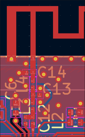
I have designed everything in KiCad, and have the KiCad docs on GitHub (https://github.com/bvizanko/nrf54-soil-moisture-sensor). I have attached a pdf of my schematic and a screen capture of the top layer.

Please let me know if you need clarification. Thanks!

Parents
  • Hi,

    • The nRF54L15-QFAA will not pass regulatory certification on a 2 layer board, it is sensitive to the distance to the GND layer under the ANT pin. If this distance is more than 100um the board will radiate harmonics above the FCC limits.
      If you are planning on getting this board certified, you'll need to switch to a 4 layer board.
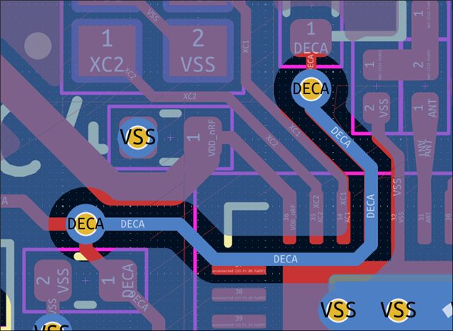
    • Another complication with just 2 layers is the routing of the DECA/DECRF connection, if it's routed directly under the XC1 and XC2 lines it can introduce noise to the clock signal which can impact the radio performance. On a 4 layer a internal GND layer would shield the traces, but on a 2 layer board the DECA/DECRF trace must be routed differently. The best option is probably to route it like this:
    • The antenna tuning capacitor C15 seems to be missing from the layout:
    • The filter components(C11 and R1) on the reset line must be moved as close as possible to the pin. These are required for filtering RF signal coupled from the ANT pin to the reset pin. If the filter is too far from the pin the reset trace will act as a antenna increasing the radiated RF noise.
       

    Other than these points the schematic and layout looks OK.


    Best regards,

    Bendik

  • Hi Bendik,

    I hope you are well. Are these observed radiated emissions on the nRF54L15 also on the CAAA package? I am designing a 6-layer rigid-flex to be required as under 0.6mm thick due to space constrain on a smart ring, and my current dielectric layer between top and inner layer 2 is 0.17mm.

    I look forward to hearing from you.

    Kind regards,

    Oliver

  • Hi Oliver,

    No, it's only a issue on the QFN package, the WLCSP package is not affected.


    Best regards,
    Bendik

Reply Children
No Data
Related