Hi,
We are migrating from NRF52840 to NRF54L15 (QFN48).
I am using nrf54l15-qfaa-reference-layout-0_8 as reference but really struggle to understand some design choices.
Aplologies if these questions have been answered before my search couldn't find what I was looking for.
It would be very helpful if somebody from Nordic hw team could look at questions below:
1. C13 (reset pin bypass) is 3.9pF. This value is less than parasitic pin capacitance - should it be 3.9nF?
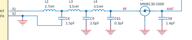
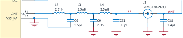
2. C11 (last cap in antenna matching network) is 0.3pF. A u.FL connector pin geometric tolerances or a speck of dust would introduce same order of magnitude error.
3. The reference design is 4 layers. I have seen mentions of previous 8 or 6 layer designs. Is 4 layer a latest recommendation?
4. It seems that C1-FB1-C2 are a just a filter for DECD output, and DECA and DECRF are locally bypassed by C12 and C5. Meaning that the track at the bottom layer connecting DECA and DECRF pins should probably be replaced with a normal power island on Layer 2?
5. Given that C9 is referenced to the bottom ground and copper windows under RF circuitry, bottom layer is a primary RF ground. So why RF ground has tracks but not Layer 2 for example?
6. What is the rationale of having 3 ground layers in a 4 layer pcb?
7. With a window under RF circuitry it looks like RF clearances were calculated for the bottom ground referenced waveguide. Is that correct? I have measured 0.15mm clearace along the RF path and 0.16mm around ground island.
8. The stackup is 1.56mm with 1.2 core and not impedance controlled. Was it intentionally selected or just being a simplest option?
9. What is the rationale of having a ground island C9 connects to? Is it just becuase of 1.6mm stackup? Yet C11 connects to RF ground using nearby vias.
10. What was the rationale to migrate to 0201 parts from 0402 before? It is a same working frequency/wavelength as NRF52.
11. What is the drive strength for X1 and X2 crystals?
Thanks. Your commects will be greatly appreciated.