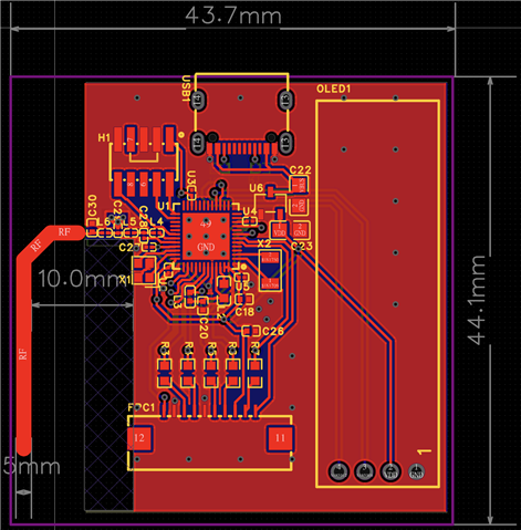
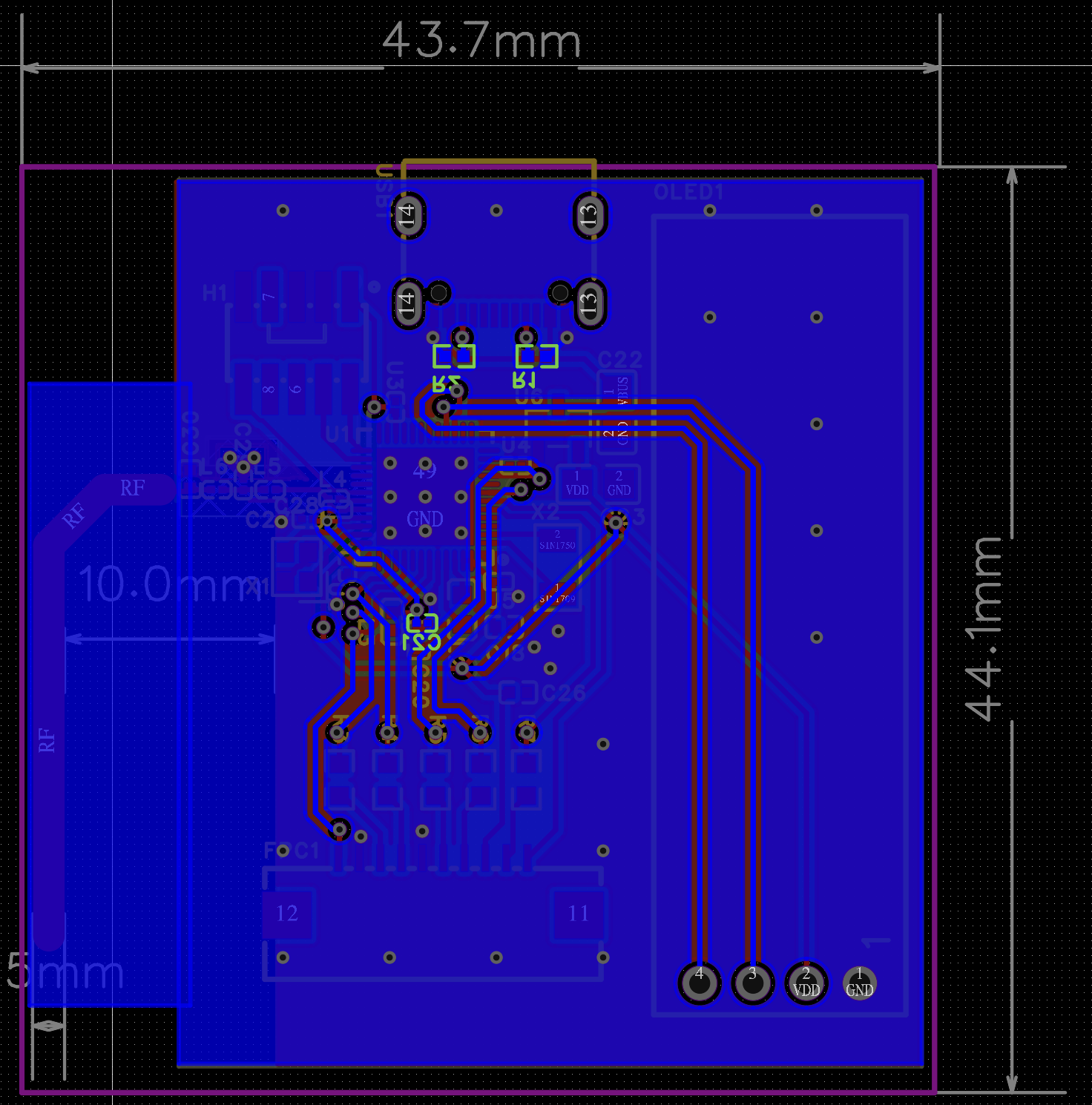
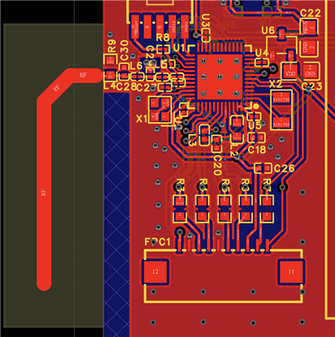
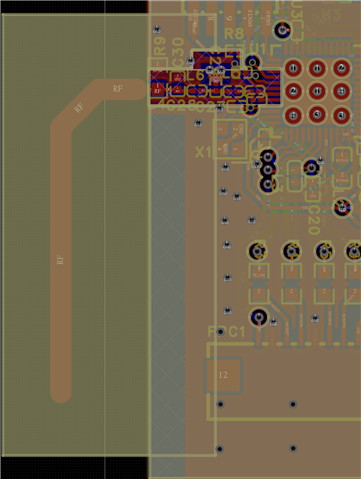
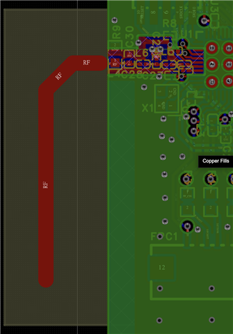
Hello this is my first time designing nrf series. and i want some feedback of my board design and rf circuit
Thanks in advance for your time and suggestions.
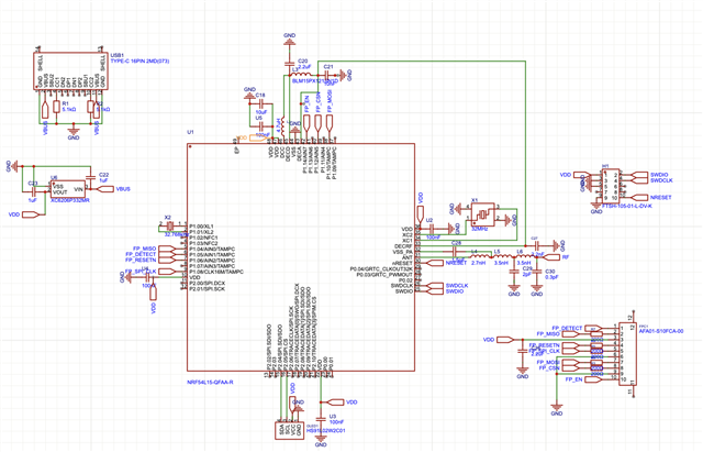
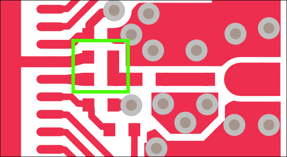
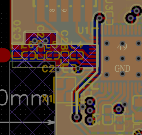
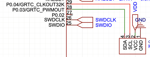
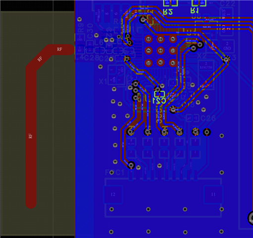
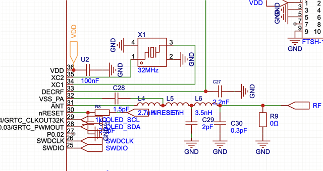
these are my circuit and bom
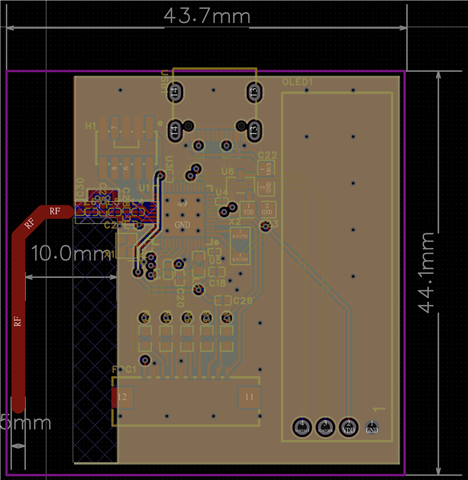
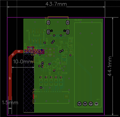
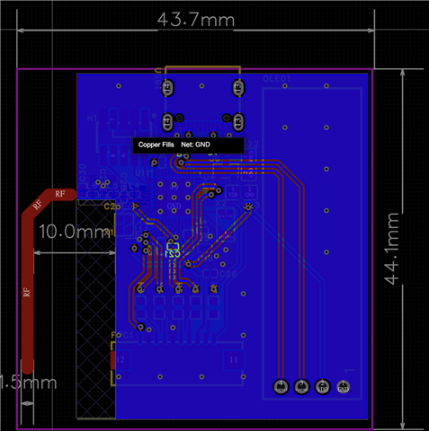
Hello this is my first time designing nrf series. and i want some feedback of my board design and rf circuit
Thanks in advance for your time and suggestions.
these are my circuit and bom