Question about chip antenna placement on a PCB

Hi,

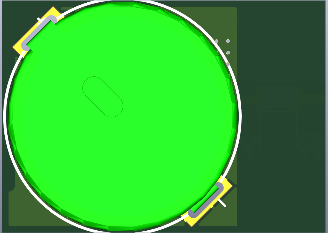
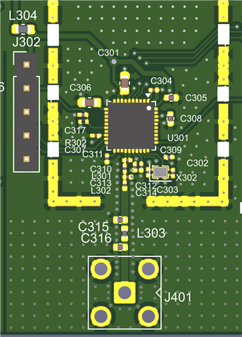
I’m planning to use a chip antenna that meets the attached specifications.
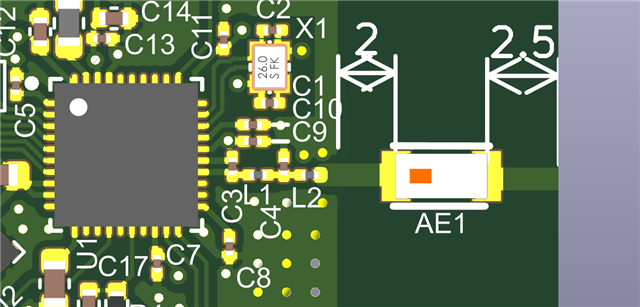
I’m not very familiar with RF hardware, and I’ve only just started using CAD.
I placed it according to the specifications, but I’m not fully confident about the layout.
Could you please review it?

A CR2032 battery will be mounted on the back side.
For additional RF tuning between L2 and the chip antenna, is an additional pi-network required?

BR
Paul

Parents
  • Hi Paul,

    The layout of the antenna looks OK

    For additional RF tuning between L2 and the chip antenna, is an additional pi-network required?

     L1, L2 C3 and C4 are the radio matching and filtering circuit, it can not be used for antenna impedance matching.

    From the snippet from the antenna datasheet you can see that a Pi network consisting of 2 shunt capacitors and one inductor is recommended:

    As a starting point the capacitors can be NC/DNP while the inductor can be replaced by a 0 Ohm link. The values of these components must be determined after the board is produced and the impedance of the antenna is measured using a VNA.


    A CR2032 battery will be mounted on the back side.

    Where is the battery placed in relation to the antenna? Is it directly behind it?


    Best regards,

    Bendik

Reply Children
Related