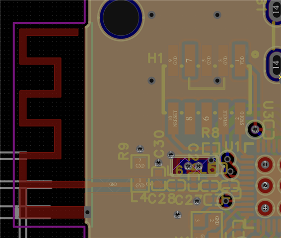
Hello this is my first time making rf circuit and i would like to get feedback on this circuit with nrf54l15.
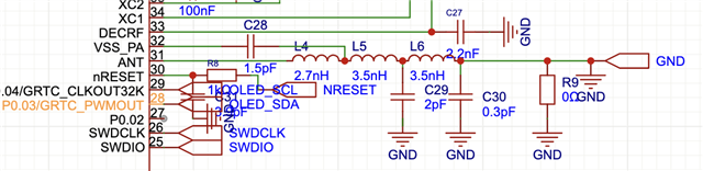
I used Texas_SWRA117D 2.4GHz IFA antenna.
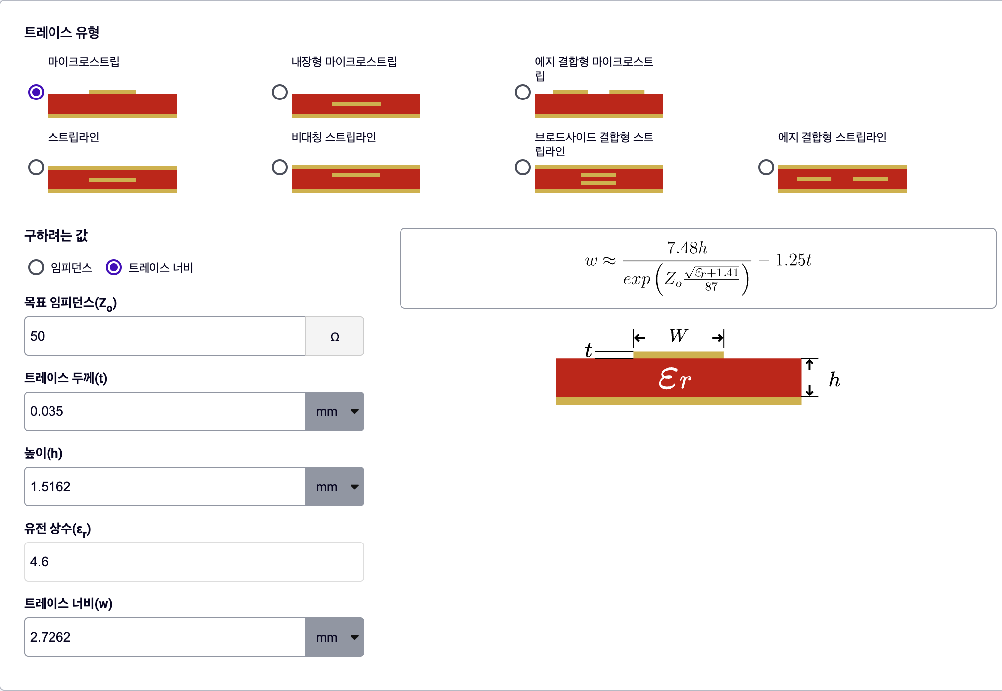
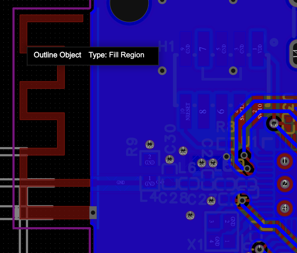
Calculated impedance with inner 1 layer's gnd
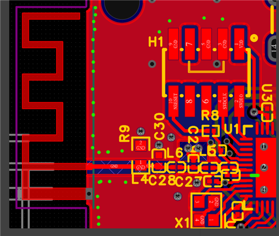
Top layer
Inner1
Inner 2
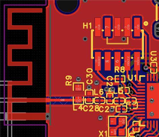
Bottom
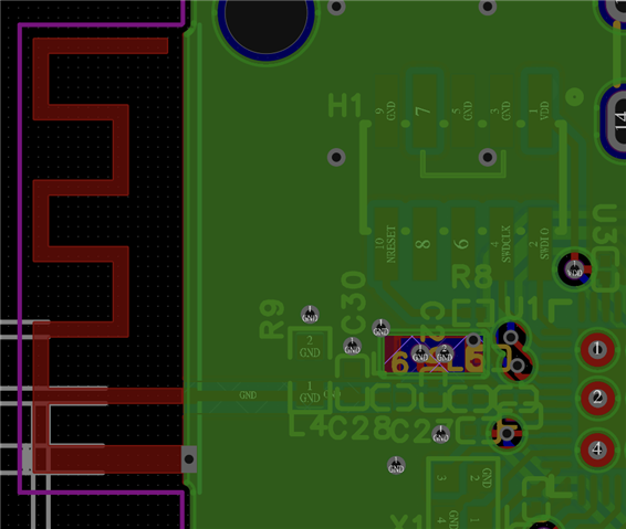
Hello this is my first time making rf circuit and i would like to get feedback on this circuit with nrf54l15.
I used Texas_SWRA117D 2.4GHz IFA antenna.
Calculated impedance with inner 1 layer's gnd
Top layer
Inner1
Inner 2
Bottom