Hello,
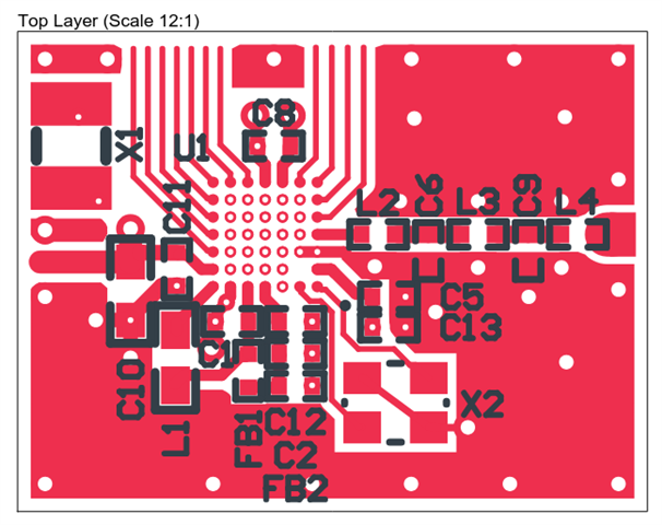
In document nRF54L15_qfaa_4L_config1_pcb_reference_layout_0_6 there is a representation of the PCB with 4 layers. The GND of C9 is not connected on the top layer, nor on the inner layers, but only on the bottom layer using vias.
In document nRF54L15_caaa_config1_pcb_reference_layout_0_3 , ithere is an 8-layer representation: the GND of C9 is still not connected on the top layer, but it is connected to all the inner layers and to bottom.
For a 6-layer PCB, which configuration is correct? The one where only the top is connected to the bottom, or the one where the top is connected to all the layers?
Thanks in advance.
3146.nRF54L15_caaa_config1_pcb.pdfnRF54L15_qfaa_4L_config1_pcb.pdf