Measurement issues with PPK 2 on nrf52833 dk

Hi,

While testing, I ran into multiple problems when measuring the current consumption with the PPK 2 on the nRF52833 dk.

For all measurements the Blinky + Bluetooth demo program was used.

1.

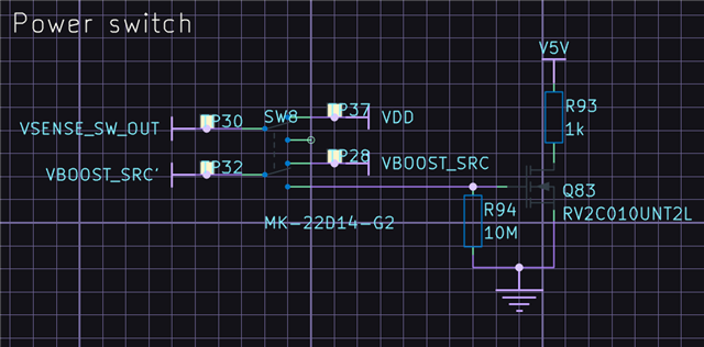
When the PPK is used as a source, connected the upper pin of P22 and gnd to P21, the LEDs are dimmed.
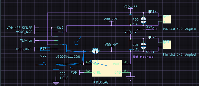
SW9 is on VDD and the power output is set to 3.3V
If SW8 is on and SW9 is put on either LIPO or USB, the LEDs go to full brightness.
When SW8 is off, switching to LIPO or USB will cut power.

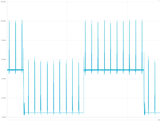
Current with dimmed LED, VDD: 3.3V, SW8 OFF, SW9 VDD

Current with full brightness LED, VDD: 3.3V, SW8 ON, SW9 LIPO

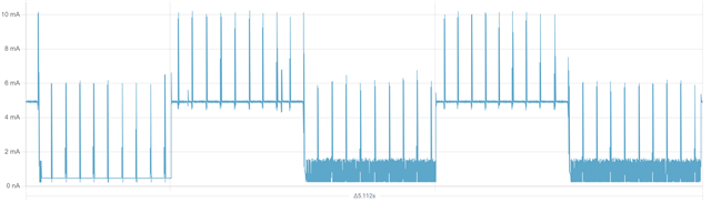
Current with SW8 from off to on, VDD 3.3V, SW9 VDD

Funnily enough, when switching SW8 to on, the measurement becomes much more noisy, since most likely other ICs are now powered.

2.

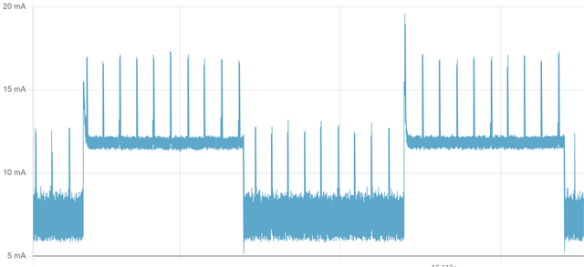
When the PPK is used as a meter, with power coming from the Debug USB (not nRF USB) the current measurement does not make sense

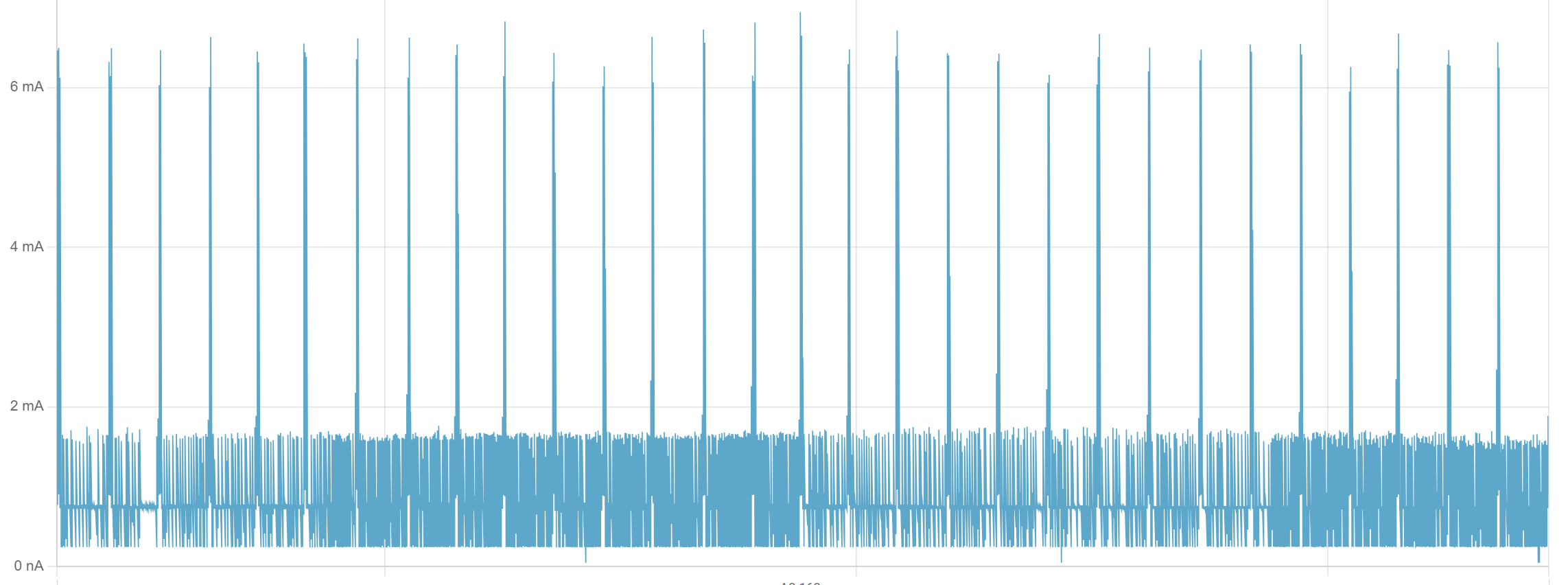
Current, LED on/off, SW8 on, SW9 VDD

The phase with less noise is when the LED is off, the phase with more noise is when the LED is on

Additionally, every LED transition (hi to lo and lo to hi) causes the LED from the debugger IC to flicker.

So now to the specific questions:
Why does the weird behavior in 1. happen?
Why does the ppk in meter mode not measure the led current BUT does suddenly have more noise when the LED is on?
The average current in the LED low state in image 1 is around 560 to 600µA but the average current in image 4 is 800µA, ... why?
Is there a chance that this behavior is due to a broken ppk oder dk (the "problems" described were there since the dk and ppk were fresh out of the box)?
Why does the debugger led flicker on transitions (any proper decoupling, which I assume is present, should mitigate that)?

Thank you for any help

  • Thank you for the answer

    When I tried replicating the measurements I noticed that the usb port (thank you, cheap usb hub)I was using for the devkit was broken / did not deliver 5V.
    I do not know how I missed that and I apologize for wasting your time making you search the solution, when the interface USB did not receive power.

    My guess is, that using the PPK as a standalone power source is not recommended and will probably result in the irregular / weird behavior I described.
    (*Edit It does explain not measuring the led current (2. in the initial post), VDD is most likely sourced by the interface usb)

    However I am still curious why this behavior did happen so here is my guess:

    Since the nrf52833 does have an internal LDO, VDD_HV and VBUS_nRF do most likely have a connection to VDD_nRF

    meaning VDD_HV' / the net colored and
    VBUS_nRF' do have a voltage applied to them.

    (the Load switch is not bi-directional, the body diode of the p-channel mosfet does not block voltage from Vout spreading to Vin)

    The nets to the left of SW9 and VBUS_nRF' are connected to the source of the boost converter

    Now depending on how SW9 is positioned either only VBUS_nRF' or both VBUS_nRF and VDD_HV' are connected to the boost source. This would explain the increase in LED brightness, since connecting vbus and vddhv in parallel could supply more current than just vbus

    The power switch SW8 does have the option to either connect VBOOST_SRC' to the actual input of the boost converter or enabling a pulldown on the 5V net and cutting power from the converter.
    This would match the LED turning off, when SW8 is in "off".

    The boost will feed the buck converter for VDD.

    BUT this does not answer, why the LED has a supply, when SW8 is on

    If SW8 is off and SW9 is (only) on VDD, the LED does also emit light. (VDD_nRF' which is connected to VSRC_NRF which is connected to VDD is most likely powered, but this net should be floating)

    And this assumption I made is most likely wrong, since I still do not fully understand the schematic.

    Thank you for your time 

    BR,
    Tobias

  • Hello Tobias,

    Actually the net is not floating when you have SW8 off and SW9 is et to VDD is the SW6 is on the default position. The net is being back powered through the nRF53833's internal diode. It sits at roughly VDD potential.

    The first part of the diagram is U19, an operational amplifier which feeds to base of Q80. Together they are follower who actively forces the rail to the reference voltage. Even we think the buck regulator path is off, but actually not. This loop can hold the node at VDD.

    Later you can see two load switches and SB39 solder which gives multiple feed paths. So, even the SW8 switch is off, the rail is being held up by either the opamp follower or VSupply Bypass, that can power the debug MCU and also the led. 

    You need to set SW6 to the nRF only to disconnect this rail. You can also check SB39 if it is soldered. Then it will couple VSUPPLY to the rail regardless of the position of the switch SW6. So, it needs to be open. 

    You can try this and measure the current again?

    Thanks.

    BR
    Kazi

Related