Hi Nordic Team,
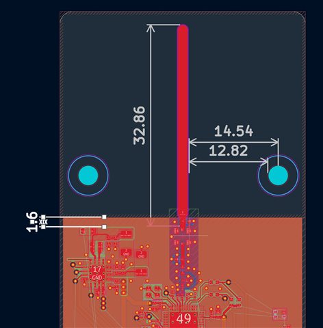
I'm developing a quarter wave PCB antenna, based on Nordic's white paper on the topic, for the nRF54L15.
I've two concerns on how features around the antenna may affect its efficiency.
First, I've to place some mounting holes and we already have a defined enclosure. As seen in the picture, they holes will be around 13mm away from the antenna, the screws will be plastic or we will use some kind of rubber holder. I'm not sure how this feature could affect the antenna and if it's worthy considering another enclosure for the prototype.
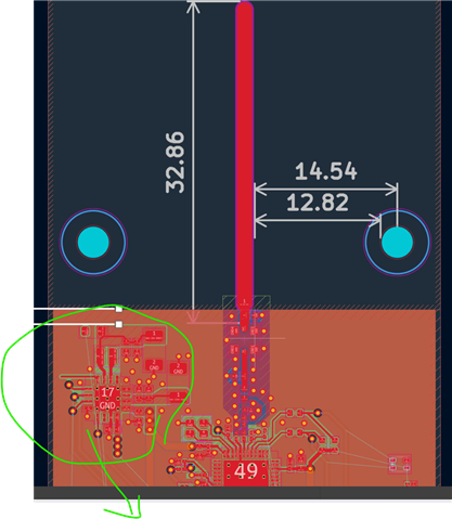
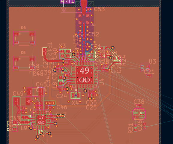
Second, we are using a pm2100 for PM and the circuity it's just 1.6 mm away from the keep out zone and I think it may be disturbing the GND plane. We used the suggested stackup of solid GND on bottom and keep out zones for under the RF zone for L2 and L3. We could move the circuity downwards but wanted to understand more deeply how this is possibly, if it actually is, affecting the antenna.
There are tunning networks available for both the antenna and the radio but my doubts are more not if it could affect the tunning but rather an unrecoverable loss on efficiency. Stitching vias are pending but consider.
Any orientation or guideline would be appreciated.
Best,
I