Can I reduce the thermal pad size for the nRF52840 (aQFN)?

Can I reduce the thermal pad size for the nRF52840 (aQFN)?

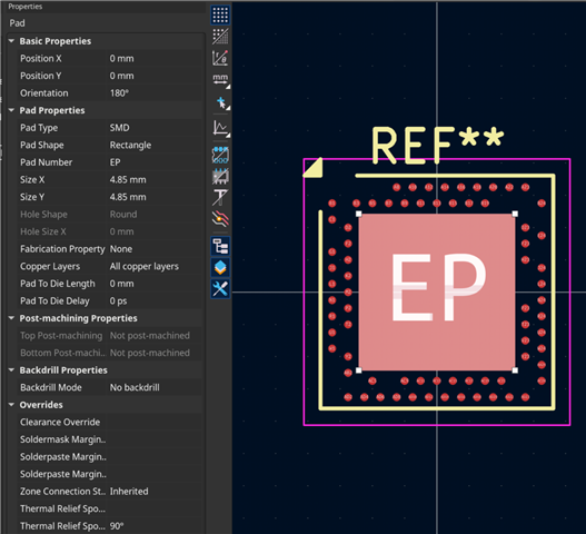
Currently the thermal pad is 4.85mm x 4.85mm, but in order to facilitate breaking out all the inner pads, reducing the thermal pad size would be greatly beneficial 

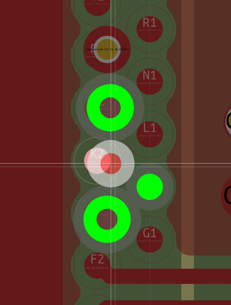
For the current design, for the row of 7 pads on the top-left side it is impossible to break out a pad with out fab's capabilities. So I would like to reduce the thermal pad size to make room. But by reducing it's size would there be fabrication problems? (We have EING and eproxy filled vias)

Thanks

Parents
  • Hello,
    If I understand you correctly your assembly factory or PCB manufacturer says they cannot support the resolution and steps used in the nRF52840 aQFN reference layout?
    What changes for the steps and resolution are you looking for? 
    We can't really recommend reducing the size of the die pad in the foot print, but it could be done as long as you make sure that the routing isn't shorted against the die pad and avoid routing high frequency or clock signals under the die pad.
    I'd be more encouraging in finding a different assembly house that can work with the tolerances needed to follow the reference layout.
    Best regards
    Asbjørn
Reply
  • Hello,
    If I understand you correctly your assembly factory or PCB manufacturer says they cannot support the resolution and steps used in the nRF52840 aQFN reference layout?
    What changes for the steps and resolution are you looking for? 
    We can't really recommend reducing the size of the die pad in the foot print, but it could be done as long as you make sure that the routing isn't shorted against the die pad and avoid routing high frequency or clock signals under the die pad.
    I'd be more encouraging in finding a different assembly house that can work with the tolerances needed to follow the reference layout.
    Best regards
    Asbjørn
Children
No Data
Related