

Hello,
I am developing a custom board using the nRF9151 and comparing the following Nordic sources:
- nRF9151 DK PCA10171 hardware files, version 1.0.0 / board revision 1.0.1
- Current nRF9151 Product Specification
- Current nRF9151 Hardware Design Guidelines and recommended application schematic
I found two apparent discrepancies and would appreciate clarification on which implementation Nordic recommends for a new custom design.
1. COEX0 load capacitance
The current COEX hardware-design guidance states that the total load capacitance on the COEX pins, including routing parasitics, must not exceed 50 pF.
However, the nRF9151 DK schematic appears to connect COEX0 to discrete capacitance whose nominal total is greater than 50 pF.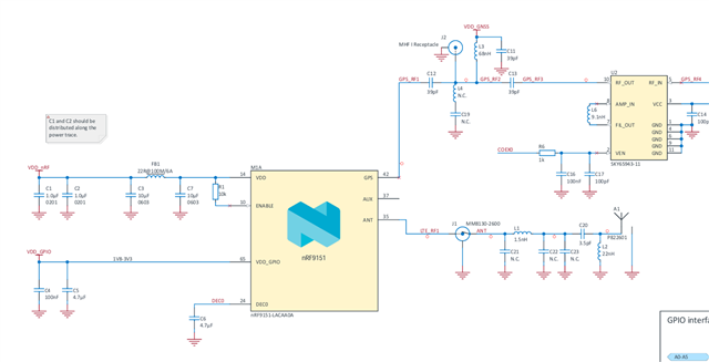
Could Nordic please clarify:
- Does the limit depend on how COEX0 is used—for example, coexistence signaling versus external GNSS LNA control?
- Is the DK implementation a validated exception that should not be copied into a different layout?
2. VDD filtering and decoupling
The current recommended nRF9151 application schematic uses:
- 1 µF + 1 µF on the source side of the VDD ferrite bead
- 47 µF + 10 µF on the nRF9151 side
- A 22 Ω at 100 MHz, 6 A, low-DCR ferrite bead
The VDD capacitor values and/or their placement around the ferrite bead appear different in the nRF9151 DK schematic: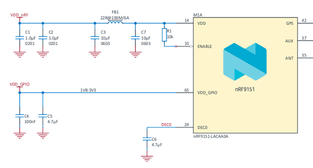
Similarly, the Thingy91x shows something different as well: 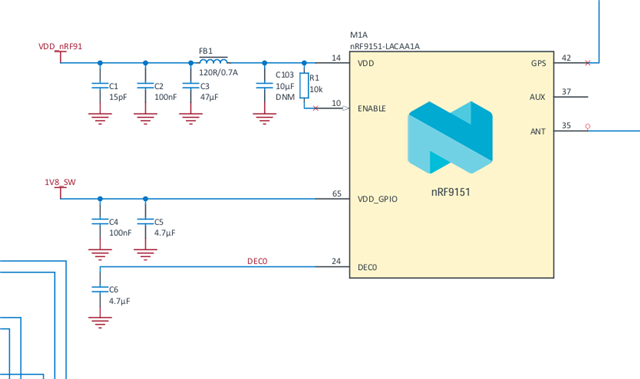
My questions include:
- Is the application schematic the preferred baseline for new product designs?
- Which topology should be followed when powering nRF9151 from an nPM1300/VSYS rail and a single-cell Li-ion battery?

