

Hi Nordic,
We are building a custom board using the nRF9151 LACA.
We see a back-powering issue between the GNSS antenna bias rail and VDD_GPIO.
Setup:
-
VDD_GPIO is configured/supplied as 1.8 V
-
VDD_GNSS is 3.3 V
-
When VDD_GNSS is enabled, VDD_GPIO rises from 1.8 V to about 2.8 V
-
When VDD_GNSS is disabled, VDD_GPIO returns to 1.8 V
-
Modem firmware version: mfw_nrf91x1_2.0.4
For reference, our design was based on the nRF9151 DK SMA hardware files.
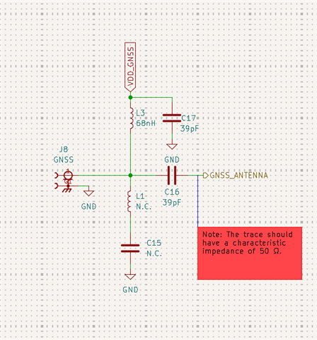
Our GNSS circuit uses an SMA connector with VDD_GNSS bias injected through an RF choke into the GNSS antenna feed. The nRF9151 GPS pin is connected through the GNSS RF/matching network, similar to the nRF9151 DK SMA design.
Our custom board:
nRF9151 Dk SMA: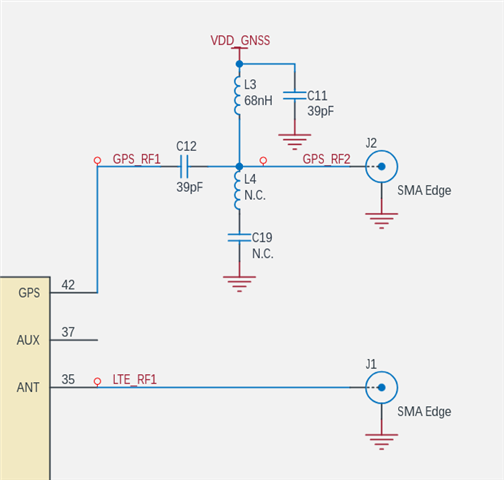
We cant see any difference between our and your design. Is there something we are missing?
