Hello.
The matching network of my design is exactly the same as the reference guide. I am using a 50 ohm ceramic chip antena on the output. I have 2 questions.
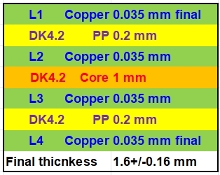
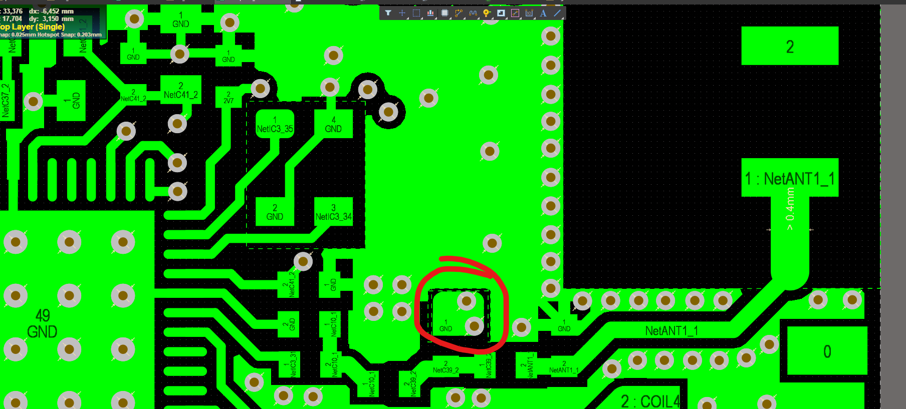
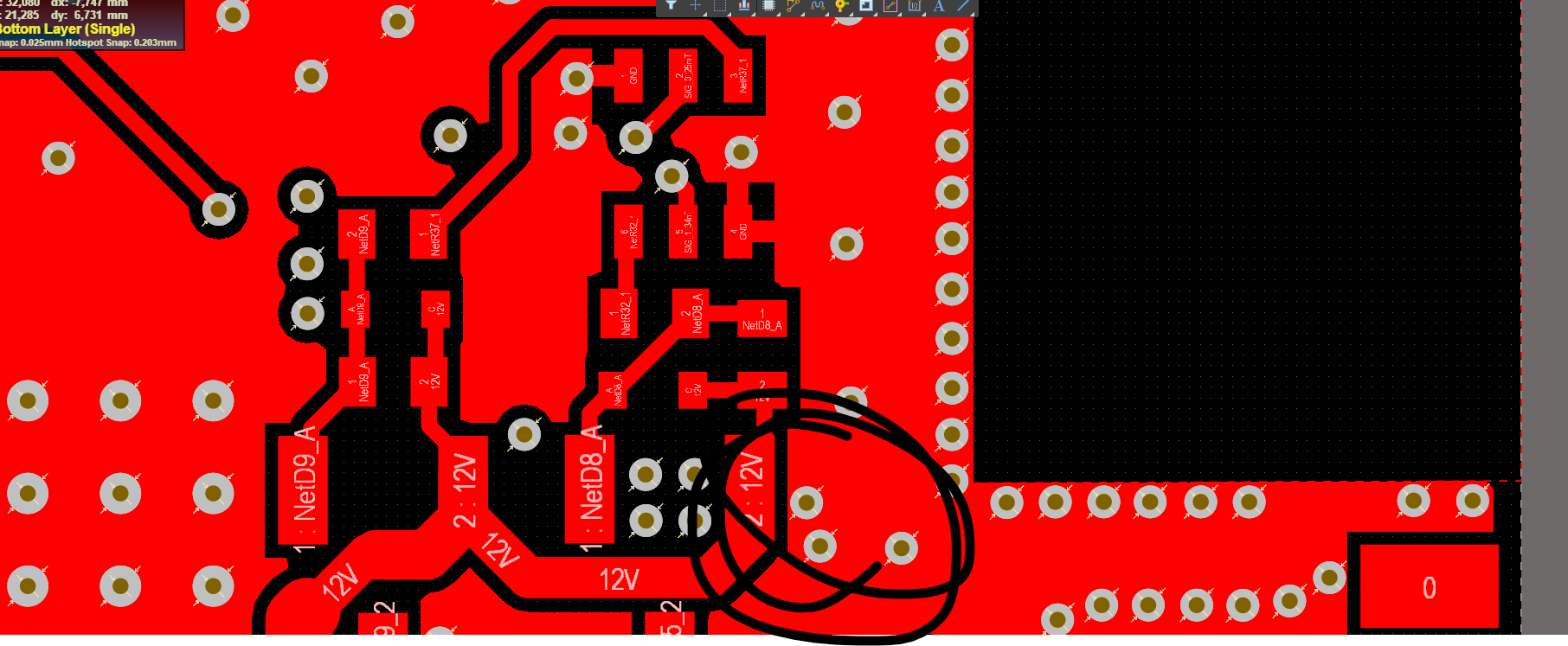
1.Reference design tells us to ground the single capacitor only to the bottom layer. My design has very poor GND coverage on the bottom layer, so i am wondering, if this rule still applies to my design. It is a 4 layer board with 2nd layer being GND plane.
Top layer:
Bottom/Last layer:
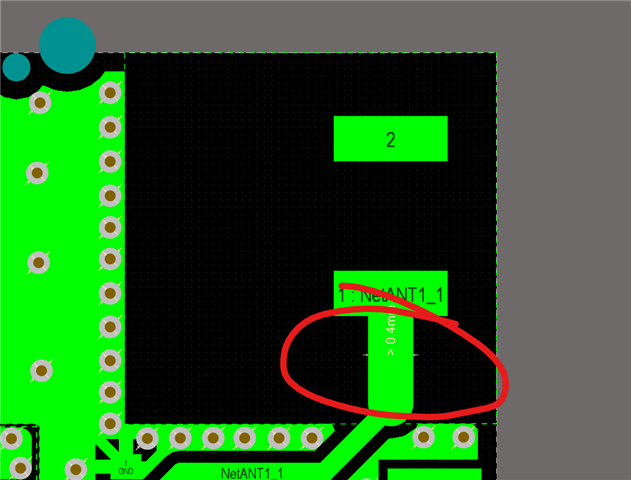
2. Reference design for the ceramic chip antenna has the last part of the trace inside the polygon cutout significantly widened, so I followed it. However, I'm wondering why the trace becomes so wide. Is it because achieving a 50 Ω impedance inside the polygon cutout requires a much wider trace?
How do you even calculate the trace impedance if there is no ground plane beneath or beside it? Elsewhere on my board, the calculated trace width after the matching network is 0.35 mm.
Thank you.