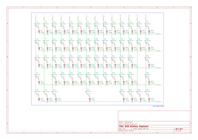
For context, I already made V1 of this keyboard and it worked as expected. It flashed, turned on, and worked fine as a keyboard. However, I identified multiple places where fixes could be made. This design addresses most of the pain points that I had. This is a wireless keyboard design using a nRF52840 (aQFN) and nPM1300 (QFN) for power management. In this version, there is a new daughterboard that has the new power switch and the USB-C connector on it which will allow the new gasket mount configuration. I have attached both board files to make it easier to review. I am avoiding via in pad and extremely small vias for cheaper manufacturing, and I do realize that the fanout is a little messy. I am not sure if that is a large issue though.
I would love feedback on the following and more:
- Tolerances/Trace Spacing near the nRF52840. It is within JLCPCB limits however I am not sure if things are still too close. Does the fanout need to be reworked in any way?
- RF - Using standard Nordic recommended network, but I am not sure about the new UFL setup. I did this so the antenna can be routed up to the top of the board. Will the current setup work?
- Grounding/Return Paths - I am not sure whether there is enough grounding near the chip. I was able to keep inner layer 2 completely clear but inner layer 1 got cut up pretty badly. Is it ok as is?
- Manufacturability
- ESD - Is the current ESD setup for the daughterboard fine?
- Any other issues
Stack up:
-
Sig / Gnd Pour
-
Gnd Plane
-
Gnd Plane
-
Sig / Gnd Pour