Hello,
I am developing a mouse product using the nRF54LM20A (QFN52). Several prototype boards have been built and are currently under debugging. The hardware uses an external 32 MHz crystal with internal‑configured load capacitors.
I have observed that on some boards, the crystal fails to start oscillating when powered by battery only. However, once USB power is plugged in (USB power detection triggered), the crystal starts normally. After that, if the USB cable is unplugged and USB power is removed, the crystal keeps oscillating properly.
To summarize: the crystal cannot start up without USB power, but it can start normally when USB power is present. Could you please advise which configuration setting may be causing this behavior? Thank you!

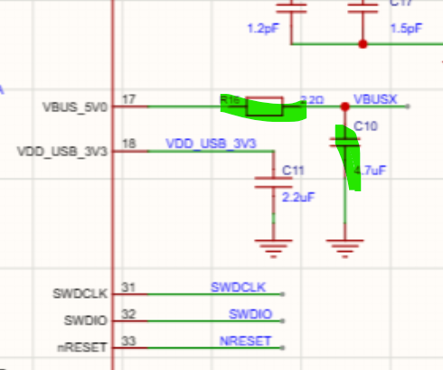
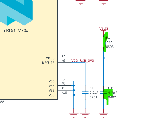
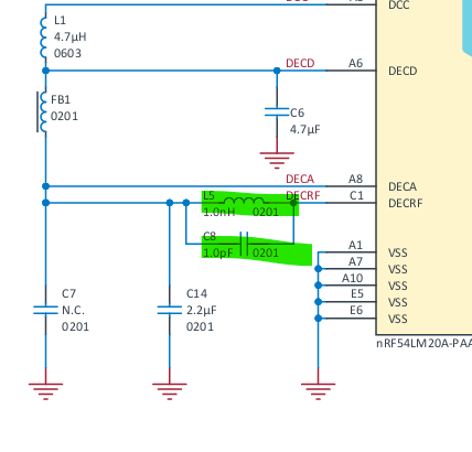
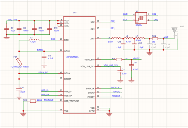 the attached is schmatic