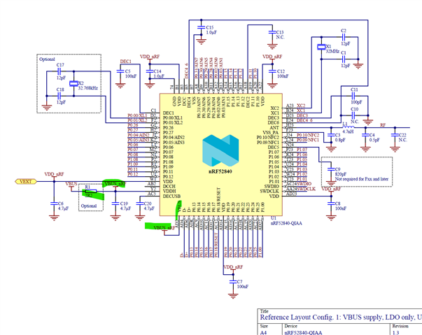
We are designing an nRF52840 (Ebyte E73-2G4M08S1C module) into a battery-powered wearable, USB device only, Full-Speed, sink-only Type-C with 5.1 kΩ Rd on both CC pins. We are trying to establish whether a design of ours genuinely violates a spec limit, or whether we are reading the limit too literally.
The limit
nRF52840 Product Specification v1.11, §5.3.8.6 (p.157) gives RSOURCE,VBUS = 6 Ω max, described as including the cable.
Our situation
For safety reasons the module's VBUS pin is not connected directly to the connector. There is a local 5.0 V LDO between them, so the module's VBUS pin is fed from a regulated source rather than from the bus:
USB-C VBUS ── [protection] ── LDO (5.0 V) ── nRF52840 VBUS pin
Because bus VBUS is 4.75–5.5 V and the LDO is a 5.0 V part, it operates in dropout essentially all the time, where it behaves as its own R_DS(ON): 4.90 Ω typical / 10.0 Ω maximum. With board resistance that is about 5.13 Ω typ / 10.33 Ω max between the connector and the module's VBUS pin — over the 6 Ω limit at the maximum corner, before any cable.
What we have already worked out
- We initially dismissed this by converting the resistance into a voltage drop. That was the wrong move: the spec is written as a resistance, not a drop.
- We also initially assumed the VBUS pin draws almost nothing. That was wrong too. §5.3.2 (p.86) describes VBUS feeding a dedicated internal regulator that powers the D+/D− PHY and pull-up, and §5.2.1.10 gives IUSB,ACTIVE,VBUS = 2.4 mA — about 14× the quiescent figure we had been quoting.
- At 2.4 mA, 10.33 Ω costs 24.8 mV. A fully compliant 6 Ω would cost 14.4 mV. So the entire non-compliance is worth about 10 mV of extra droop, against roughly 362 mV of headroom we have to the minimum operating VBUS.
That last number is why we are asking rather than just fixing it.
The question
What is the 6 Ω limit protecting? The PS states the number but not the mechanism, and the right fix depends entirely on which of these it is:
1. Static droop at IUSB,ACTIVE,VBUS — in which case our 10 mV of excess is plainly irrelevant and we would document it and move on.
2. Transient response of the internal USB regulator — e.g. the source impedance seen during D+ pull-up assertion, resume, or the PHY's switching load. If so, a static Ohm's-law argument is the wrong analysis entirely and we need to look at impedance versus frequency, not DC resistance.
3. Inrush or startup behaviour into the internal regulator's decoupling at attach.
4. VBUS detection / USBDETECTED event timing or threshold integrity.
5. Something about USB-IF compliance rather than device function.
Secondary question, if the answer is (2) or (3): is the limit still meaningful when VBUS is supplied by a regulator rather than by the bus? A 5 Ω LDO in dropout and 5 Ω of cable are the same DC resistance but very different sources dynamically, and we cannot tell from the PS whether the limit was written with a cable in mind specifically.
What we would do with the answer
- If it is (1), we keep the current part and record the deviation with the arithmetic above.
- If it is (2)–(4), we move to a lower-resistance regulator (we have a 3.78 Ω candidate) and, if you can say so, we would like to know whether ~4 Ω plus cable is genuinely inside the intent or whether we should be targeting something well under 6 Ω total including cable.
We would rather understand the constraint than guess at it. Thank you!