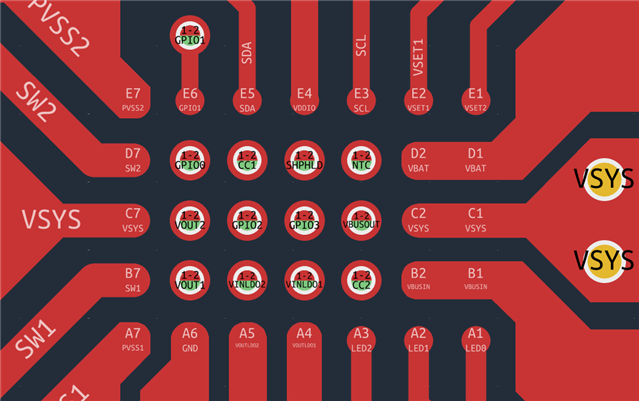
npm1300 CAAA 1.1 example layout mirrored

I'm trying to understand the npm1300-CAAA V1.1 example for configuration 1. The layout looks like this:
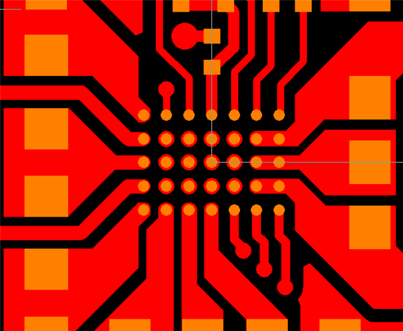
You can easily see that several pins are connected on the right side. B6 and B7, C6 and C7, D6 and D7.

However, none of those pins are shared nets in the schematic. In fact, this layout shows pin B1 connecting to L2. It is almost like the pinout got mirrored?

The AI response when I tried to submit this stated that the layout is mirrored.

Can you please confirm this is the case.

Parents
  • Hello Samuel,

    In the nPM1300-CAAA V1.1, configuration 1 example layout, the nPM1300 is not mirrored, but it is rather rotated 180 degrees with A1 in the bottom right corner. So its B1-B2, C1-C2 and D1-D2 which are connected together in this layout.


    If you are using the Altium Designer files in a PCB editor, you should be able to zoom in to see the pin assignments and verify this yourself. For example, here:


    Best regards,
    Ellen

Reply
  • Hello Samuel,

    In the nPM1300-CAAA V1.1, configuration 1 example layout, the nPM1300 is not mirrored, but it is rather rotated 180 degrees with A1 in the bottom right corner. So its B1-B2, C1-C2 and D1-D2 which are connected together in this layout.


    If you are using the Altium Designer files in a PCB editor, you should be able to zoom in to see the pin assignments and verify this yourself. For example, here:


    Best regards,
    Ellen

Children
No Data
Related