Hi,
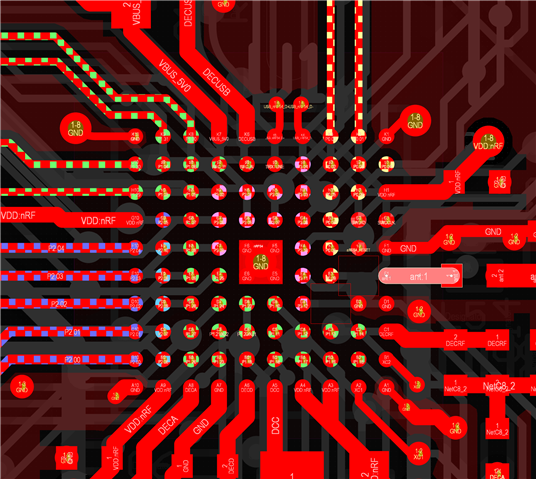
When we draw PCB, we also need to design it like your DK board? There are several square copper skins under the chip, the middle of which is grounded, and the other two staggered square copper skins are suspended without network. thank you

Hi,
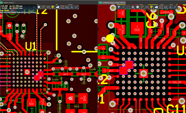
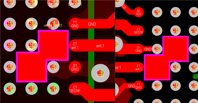
When we draw PCB, we also need to design it like your DK board? There are several square copper skins under the chip, the middle of which is grounded, and the other two staggered square copper skins are suspended without network. thank you