nRF7002 Buck Vias

The example layouts for the nRF7002 CEAA make use of microvias for escape routing, which makes sense. However, those microvias are also used to connect the ground associated with the RFBUCKVDD/PWRBUCKVDD net to a ground plane on layer 2 (pink arrow in the picture) and then other buried vias are used to connect that layer 2 to a ground plane on layer 3 (orange arrow in the picture). I understand the intention of the ground cutout on layers 1, 2, and 3 that isolate this buck section of the circuit's ground planes and why there is a ground plane on both layers 2 and 3. What I'm not understanding is why the layout doesn't just use through-hole vias to connect the top layer ground net to both layers 2 and 3 at once. This would be much cheaper to manufacture and simpler than requiring the addition of buried vias and the dozens of microvias used in stitching. 
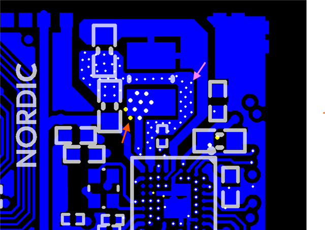
Can you please explain why this was done? Would there be any downsides to just using mechanical through-hole drills to stitch the ground planes?

  • Hi Samuel,

    I'm not sure if by through vias you mean layers 1-3 or 1-4.

    A via always has to go through an even number of layers (or odd number of substrates). On a 4 layer board, you can have vias between layers 1-4, 1-2, 2-3, 3-4. Having a via from layer 1 to 3 is generally not feasible, simply due to the lamination process used during building the PCB. These vias would require an asymmetrical stackup, which leads to warping of the PCBs. There might be some manufacturers who can do this with some workarounds, but it is not practical and certainly not the norm. And even so, buried vias would be still cheaper than these exotic vias.

    If you want to avoid blind vias, you can use 1-4 through-hole vias which are isolated on the bottom layer, something like this:

    However, we have not tested this layout so we cannot guarantee optimal performance, this is just a suggestion. The problem with this is compromise, because now the vias are breaking the continuity of the ground plane on the bottom layer. The ground plane on the bottom layer is needed for shielding, and needs to be a solid, continuous plane. Too few of these through vias will not make a good, low-impedance connection between the layers, and too many of these will disturb the bottom ground plane too much. Hence the solution with the micro and buried vias.

  • I was talking about completely through hole vias. In the case of a 4 layer board it would be 1-4 as you say.

    Your example is effectively what I am talking about. However, I'm not clear on why you say the via would need to be isolated from the bottom layer's ground. The ground plane on layer 3 of the example layouts has a cutout which limits the noise from the buck convertor, but it is not an isolated ground and is linked by vias to the bottom layer in several places.

    Can you expand on the implications/necessity to avoid linking the layer2 and layer3 ground planes to the nearby layer 4 ground? 

  • Ok, I see.

    On layer 2, there is just an isolated island, which is not connected to the ground plane, it is basically just an extra layer for the ground path on the top, effectively making the trace "wider".

    The purpose of the cutout on layer 3 is to "direct" the ground currents towards the ground pins on the chip, and also to keep these currents flowing in the inner layer. That is also why the bottom ground plane should not be connected, to avoid current flowing on the bottom layer, because that could lead to unwanted emissions. The bottom ground layer could act as a patch antenna for these currents, radiating signals that could cause interference for other devices.

    Instead, the currents are flowing in the inner layers, and they are shielded by the ground plane on the bottom. That is why the ground plane needs to be solid and continuous, to act as a good shield.

    ps. You can also see this practice on our nRF5x devices, where the shunt capacitors in the matching network are not connected directly to the ground polygon, but are grounded with vias instead. The idea is the same: we want RF current flowing in the inner layers, not on the outer ones.

Related