

Hi Nordic team,
I am planning a new design using the nRF54LM20B in the QFN52 (QFAA) package and need your help with the following.
Background: I have reviewed the published reference layout for the CSP98 (PAAA) package (see attached image). I understand that these CSP98 values cannot be reused for the QFN52 package.
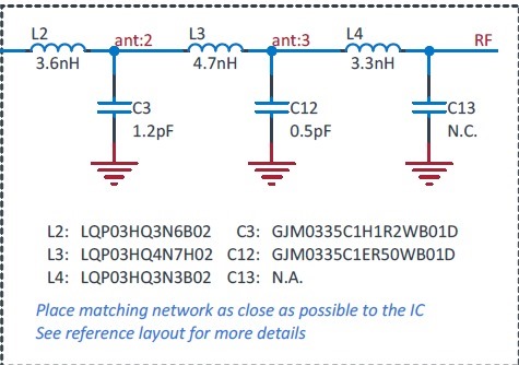
What I need:
-
QFN52 (QFAA)-specific RF reference schematic
-
Matching network BOM — component values, part numbers, footprints, and tolerances
-
Ground island design details — via count, via placement, and connection to die center pad
-
PCB stack-up and layer details
-
PCB layout files (Altium Designer preferred) if possible
Thanks and Regards
Nishant
