Can't use Nrf54L15dk to flash an external custom board ...

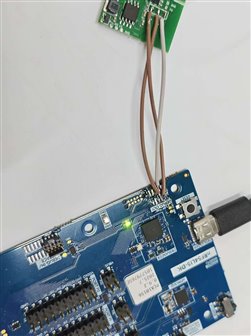
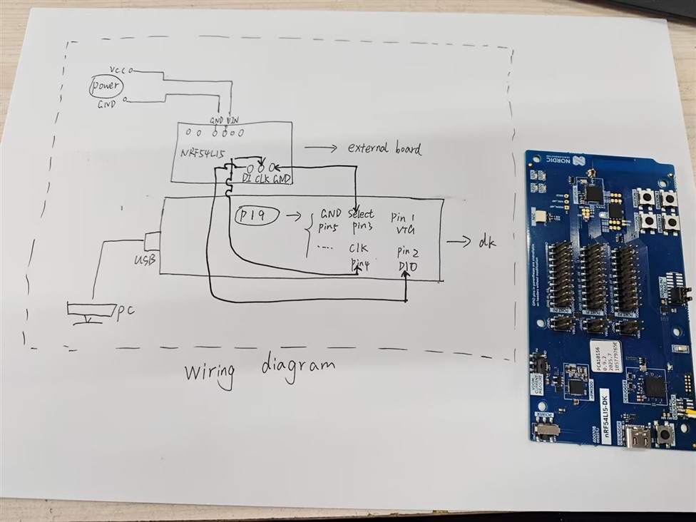
Our prototype is back. At first, I used NRF Connect to flash it, but the official PC software couldn't flash the firmware. I followed the wiring instructions: (1) connect SDIO, connect the clock line, and connect the DK board's select to the target board's GND, (2) the external board has separate power, (3) the wire length is less than 10 cm.

Burning failed with an error, as shown below:

Failed "reading readback protection status for application core". Error: code: 1, description: Generic, message: Batch task protection-get failed, Device error: Setting the debug port SELECT register failed while powering up sys and debug regions (Unknown error in the J-Link DLL (error code =-1)). This might indicate that the debug port is unavailable. Double-check device power supply and SWD lines, and ensure that SWD is not disabled
17:25:18.877        Error: Failed with exit code 1. One or more batch tasks failed: * 1057797650: Device error: Setting the debug port SELECT register failed while powering up sys and debug regions (Unknown error in the J-Link DLL (error code =-1)). This might indicate that the debug port is unavailable. Double-check device power supply and SWD lines, and ensure that SWD is not disabled (Generic) Message: Batch task protection-get failed, Device error: Setting the debug port SELECT register failed while powering up sys and debug regions (Unknown error in the J-Link DLL (error code =-1)). This might indicate that the debug port is unavailable. Double-check device power supply and SWD lines, and ensure that SWD is not disabled.
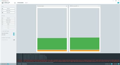
     

Then we also tried using our own pirated J-Link programmer and it failed
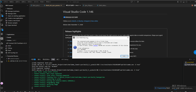
I’m not sure if these two methods are feasible. I wonder if I missed something, or if I can only buy the official J-link programmer.

  • Hi,


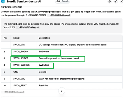
    Based on the wiring and your description, you are connecting SWDIO/SWDCLK and SELECT pins.

    Here is the pinout of the connector on the DK: https://docs.nordicsemi.com/r/bundle/ug_nrf54l15_dk/page/ug/nrf54l15_dk/program_debug/debug_out_ext_board.html


    In addition, you must ensure that your external board is powered. In your picture, it does not show any GND connection from the DK to your custom board.

    It is often recommended to power the external board with the same VDD as the development-kit.


    Then we also tried using our own pirated J-Link programmer and it failed

    I would recommend that you obtain a genuine J-Link device, as using a known clone means that you are in-breach of SEGGER's license.


    Kind regards,

    Håkon

  • Dear Håkon,

    Perhaps I did not explain clearly, which is my fault. My board is powered by an external power supply, which provides 3.3V to the chip through a buck converter, and the signal lines are less than 10 cm long. Initially, I used pins 2, 3, and 4 on P19 to interface with the external board, but programming could only reach the DK's MCU. Later, I suspected that the onboard GND might not be connected to the external board's GND, so I reconnected the two grounds, but it had no effect.

    Currently, I have two different versions of the nRF54L15 DK, with labels showing 0.9.2 and 1.0.0, respectively. The former does not have P5, while the latter has P5, but when measuring the pin header voltage with a multimeter, no voltage can be detected. Yesterday, I discussed the DK board schematic with a hardware engineer, and it was indeed confirmed that there is no voltage on P5.

    Based on this, it is impossible to directly power the external board using the DK board. Therefore, I am perplexed as to what is causing the programming to fail on the external board, allowing it to only program the onboard MCU.

  • Hi,


    VTG is not an ouput, but an input.

    Try to connect pin 1 (VTG) to your external boards VCC.


    Kind regards,

    Håkon

  • Dear Håkon,

    A couple of days ago, I also tried using an external power supply connected to the VTG pin and common ground, etc., but this operation had no effect; the programming still targeted the MCU on the DK board.

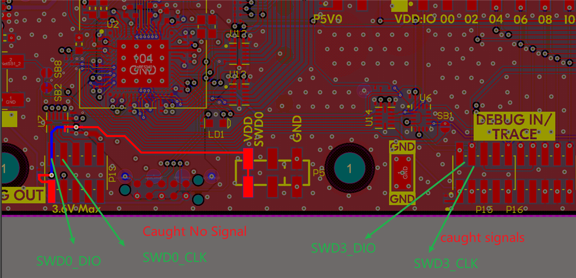
    At the same time, to verify whether the programming interface had any signal, I used a logic analyzer to capture the waveforms, with one channel connected to the board's SWD3 programming interface and the other to the external board's SWD0 programming interface. I found that during firmware programming, only SWD3 had clock and signal activity, while SWD0 did not capture any output waveforms. Therefore,

    I suspect that the key issue might lie in the switching between SWD3 and SWD0 (note: the SWD0_select pin has been connected to the external board's GND). I would greatly appreciate any good suggestions you might have.

    Best regards,

    GG Bond

  • The captured waveform results are shown in the figure.

Related