 Hi all,
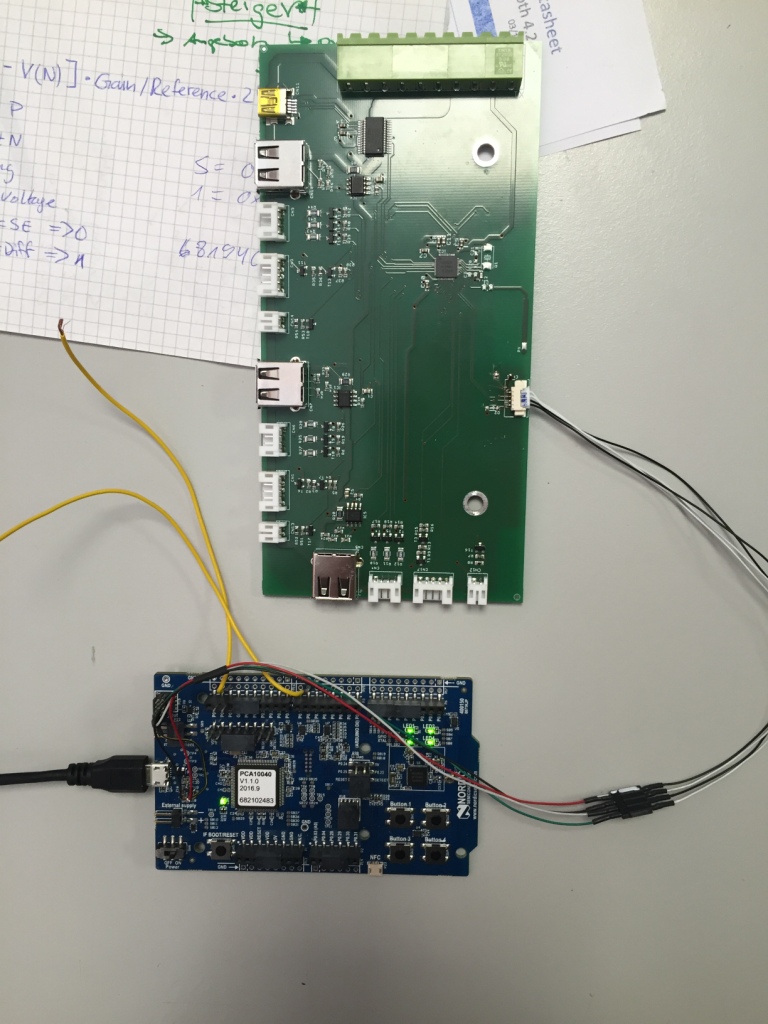
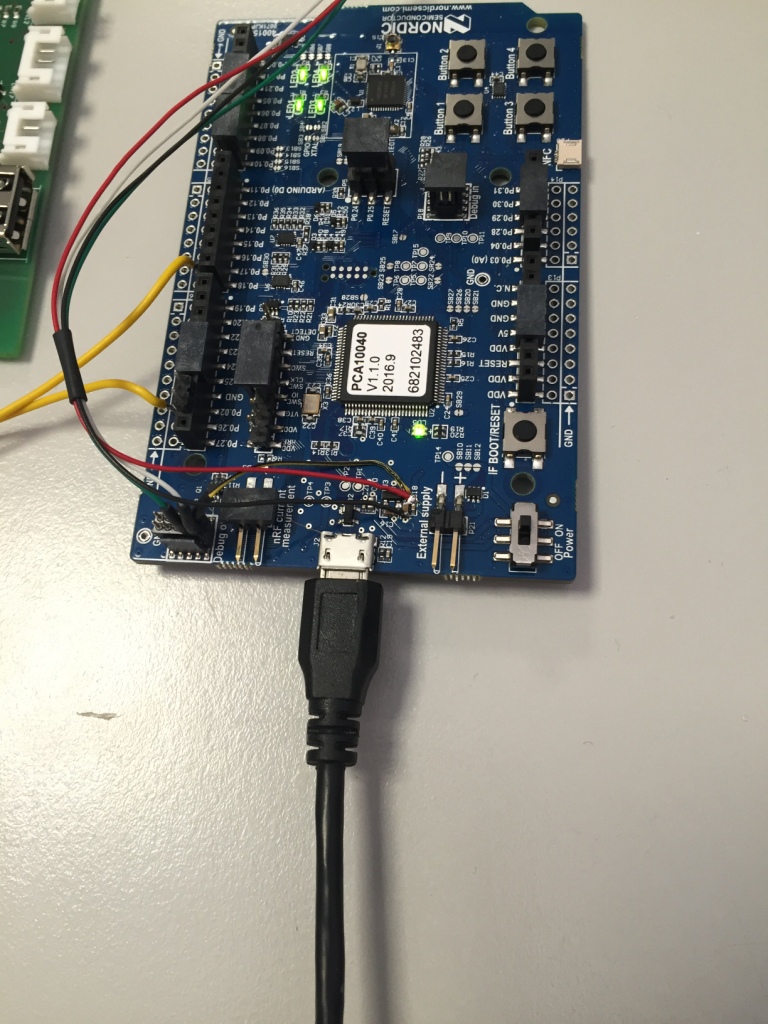
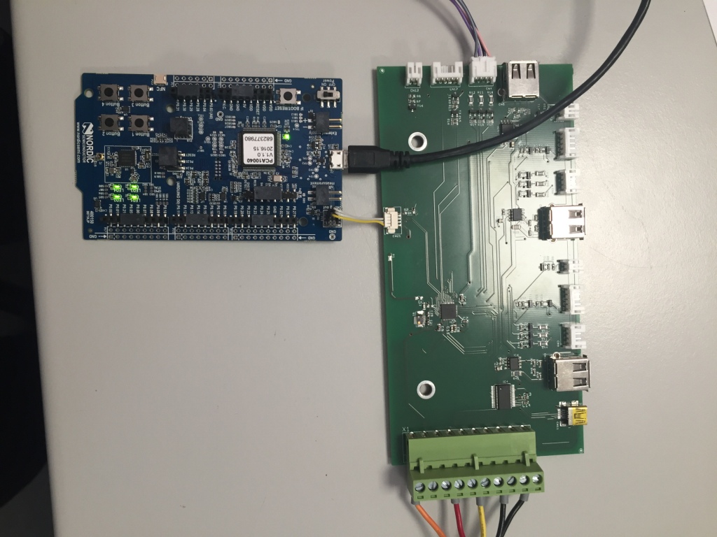
until now, I used nRF51 Chips on my board. I programed them trough the nRF51DK(PCA10028). But now I would like to work with nRF52832 Chip. I have a nRF52DK(PCA10040) and an application which is working fine on the 52DK.The application is based on peripheral examples from SDK 11. SD is not used. But when I try to download the same application on my own board with the nRF52832 Chip, will get this error:
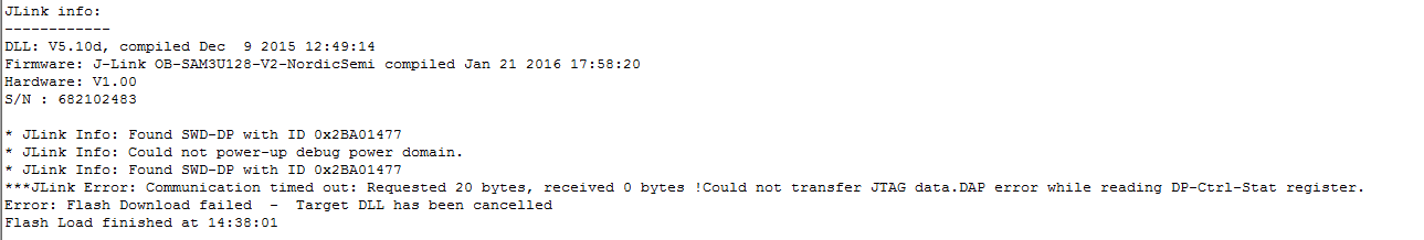
- JLink Info: Found SWD-DP with ID 0x2BA01477
- JLink Info: Could not power-up debug power domain.
- JLink Info: Found SWD-DP with ID 0x2BA01477
- JLink Error: Communication timed out: Requested 20 bytes, received 0 bytes ! Could not transfer JTAG data. DAP error while reading DP-Ctrl-Stat register.
Error: Flash Download failed - Target DLL has been cancelled.
What means: Could not power-up debug power domain? How can I fix this error?
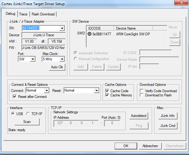
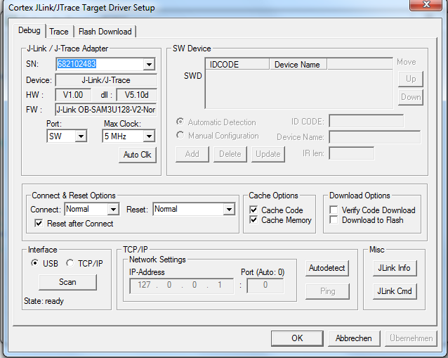
If I want to program the nRF52832 Chip is it possible to use the Segger from the 51DK, or do I have to use the segger from DK52?
Do I have to use an external crystal for programing the chip? Because I would like to work only with the internal RC oscilator.
Voltbox_Classic 1.0 BRD.pdfVoltbox_Classic 1.0 SCH.pdf
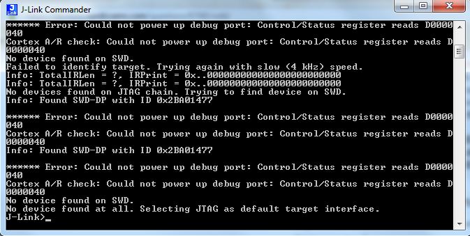
This is what I get when I want hwinfo over jlink commander