
I have been trying to adapt the following example project to work with my SPI peripheral device (LIS2DE12 Accelerometer): nRF5_SDK_11.0.0_89a8197\examples\peripheral\spi\pca10040\arm5_no_packs
My device has been flashed with S132 2.0.
Info on this peripheral is here: www.st.com/.../en.DM00153214.pdf
I am using a custom device with the following nRF to ST pin connections:
PO.02 (SS) to Pin 2 (CS)
PO.03 (MOSI) to Pin 4 (SDI)
PO.04 (SCK) to Pin 1 (SLC)
PO.05 (MISO) to Pin 3 (SDO)
I have defined these pins within nrf_drv_config.h as per docs.
#define SPI0_ENABLED 1

#if (SPI0_ENABLED == 1)
#define SPI0_USE_EASY_DMA 1

#define SPI0_CONFIG_SCK_PIN 4
#define SPI0_CONFIG_MOSI_PIN 3
#define SPI0_CONFIG_MISO_PIN 5
#define SPI0_CONFIG_IRQ_PRIORITY    APP_IRQ_PRIORITY_LOW
Note that the only other peripheral enabled is UART0 and it is not using any pins that the SPI interface is using.
#define UART0_ENABLED 1

#if (UART0_ENABLED == 1)
#define UART0_CONFIG_HWFC         NRF_UART_HWFC_DISABLED
#define UART0_CONFIG_PARITY       NRF_UART_PARITY_EXCLUDED
#define UART0_CONFIG_BAUDRATE     NRF_UART_BAUDRATE_115200
#define UART0_CONFIG_PSEL_TXD 10	// RxN Tag Config Tx
#define UART0_CONFIG_PSEL_RXD 8		// RxN Tag Config Rx
#define UART0_CONFIG_PSEL_CTS 9		// RxN Tag Config Unused
#define UART0_CONFIG_PSEL_RTS 14	// RxN Tag Config Unused
#define UART0_CONFIG_IRQ_PRIORITY APP_IRQ_PRIORITY_LOW
#ifdef NRF52
#define UART0_CONFIG_USE_EASY_DMA false
Also note that I had tried disabling DMA using:
#define SPI0_USE_EASY_DMA 0
... but found that I was only able to get a clock output during my MOSI buffer transfer but the clock was not continuing to support incoming MISO bytes. Enabling DMA seemed to fix this.
Code used for SPI init and read/write is here:
#define SPI_CS_PIN   2
#define SPI_INSTANCE  0
#if (SPI0_ENABLED == 1)
static const nrf_drv_spi_t spi = NRF_DRV_SPI_INSTANCE(SPI_INSTANCE);
#endif
static volatile bool spi_xfer_done;

static uint8_t		m_tx_buf[2];	// Control/Addr byte plus optionally used data byte for reg writes.
static uint8_t		m_rx_buf[1];	// Always just 1 data byte returned.

void spi_event_handler(nrf_drv_spi_evt_t const * p_event)
{
	nrf_delay_ms(10);

    spi_xfer_done = true;
    NRF_LOG_PRINTF(" Transfer completed.\r\n");
	NRF_LOG_PRINTF(" Received: 0x%02X\r\n",m_rx_buf[0]);
}

int main(void)
{
	ret_code_t err_code;

	err_code = NRF_LOG_INIT();
    APP_ERROR_CHECK(err_code);
    NRF_LOG_PRINTF("Altered SPI example\r\n");

    nrf_drv_spi_config_t spi_config;
    spi_config.ss_pin = SPI_CS_PIN;
	spi_config.mosi_pin = SPI0_CONFIG_MOSI_PIN;
	spi_config.sck_pin = SPI0_CONFIG_SCK_PIN;
	spi_config.miso_pin = SPI0_CONFIG_MISO_PIN;
	spi_config.frequency = NRF_DRV_SPI_FREQ_8M;			// Default 4M
	spi_config.mode = NRF_DRV_SPI_MODE_3;				// Default mode 0
	spi_config.bit_order = NRF_DRV_SPI_BIT_ORDER_MSB_FIRST; // Matches Default.
	spi_config.irq_priority = SPI0_CONFIG_IRQ_PRIORITY;

	err_code = nrf_drv_spi_init(&spi, &spi_config, spi_event_handler);
	APP_ERROR_CHECK(err_code);

    while(1)
    {
        // Reset rx buffer and transfer done flag
        memset(m_rx_buf, 0, 1);
        spi_xfer_done = false;

		m_tx_buf[0] = 0x8F;	// 1 = Read, 0 = No Addr Inc, 001111 = WhoAmI Reg Add
        APP_ERROR_CHECK(nrf_drv_spi_transfer(&spi, m_tx_buf, 1, m_rx_buf, 1));

        while (!spi_xfer_done)
        {
            __WFE();
        }

        nrf_delay_ms(100);
    }
}
There are 2 issues that I am having when issuing a read of peripheral register 0x0F (using cmd 0x8F):
-
Response data printed within the callback should always be 0x33 (the fixed value in register 0x0F), but is often erroneous.
-
Voltage levels on the clock, MISO and MOSI lines look incorrect during peripheral responses.
Relating to "1." - I repeatably read a register value of 0xFF and then the correct 0x33 (and then 0xFF again and the cycle repeats) when using the fastest Nordic SPI rate of 8 Mbps. At lower rates, inconsistent register values are read.
Relating to "2." (which may be the cause of "1."), I believe that there may be contention on the lines as indicated in scope caps.
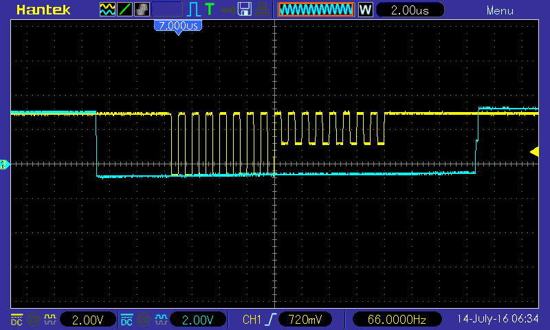
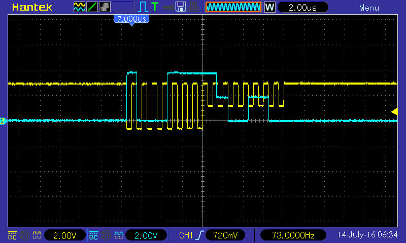
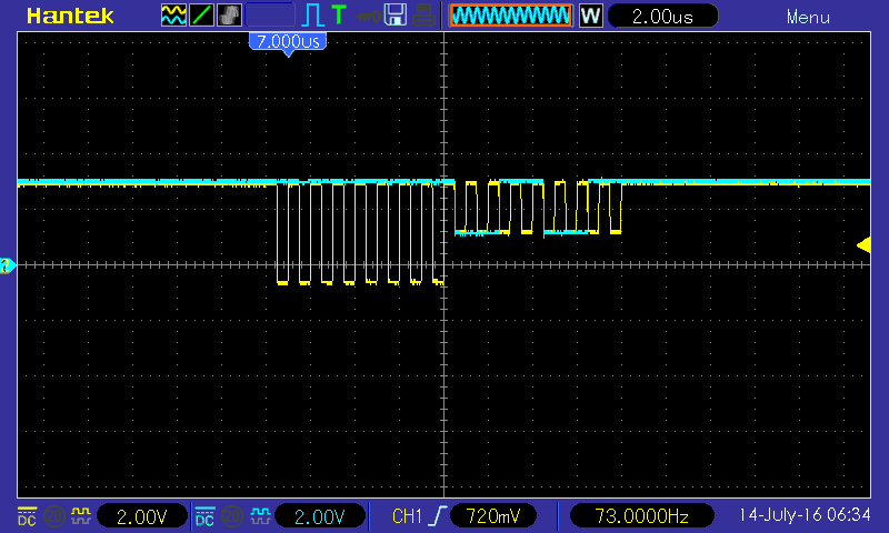
Please ignore the apparent offset from ground as there is an outstanding scope setup issue.
In this first capture, the yellow line shows my clock and the blue line shows chip select. It is driven low by the Nordic SPI driver as required.
 TagSPI_6.bmp
In this second capture, the blue line now shows the MOSI signal. It seems good until a response comes in from the peripheral and then it is driven to a strange state instead of O Vdc. The command is 0x8F (10001111) denoting read from register 0x0F.
 TagSPI_7.bmp
In this last capture, the blue line now shows the MISO signal. It's timing and indicated value is correct (byte value 0x33), but its levels seem strange.
 TagSPI_5.bmp
Could this indicate contention on the clock and MISO lines - only when the peripheral is responding to a read command over MOSI? The driver init seems to leave the MISO pin floating.
// - MISO (optional) - input,
    if (p_config->miso_pin != NRF_DRV_SPI_PIN_NOT_USED)
    {
        miso_pin = p_config->miso_pin;
        nrf_gpio_cfg_input(miso_pin, NRF_GPIO_PIN_NOPULL);
    }
Is this ok, or perhaps would a pull up help?
Changing data rates to below 8 Mbps does not seem to affect the traces, so maybe there a two distinct issues here.
Any help and suggestions are appreciated.


