This post is older than 2 years and might not be relevant anymore
More Info: Consider searching for newer posts

Can you help me checking the antenna?

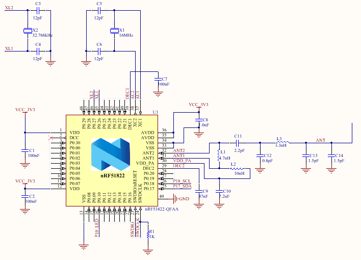
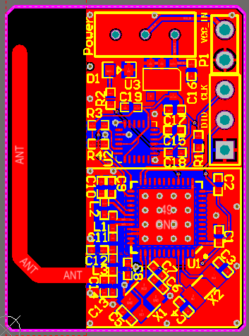
I've just finished my first layout for nRF51822, and I need a help with the attenna design. The RF part of the schematic and layout is a copy of your reference design, "PCA10004-nRFgo nRF51822 PCB Antenna Radio Module 2_0". Can you tell me are there any problems in my layout? And if it is ok, for the thickness of the circuit board or other conditions do you have any requirements.

Thank you!

sch.png PCB.png

Parents
  • Hi,

    You should use these reference design, but by the looks its seems your design is the same, except for C12 which is 1pF in the reference design. So not much to say here.

    For the antenna the lenght should be 25mm before tuning (you can read more about tuning here) and at least 5mm from the ground plane/copper on the board (it looks like yours are). The tuning capacitor C14 can be moved closer to the antenna. For tuning we recommend that you send the board to us as it should be in final product (inside correct casing etc). You can create a case on myPage and we will help you.

    The thickness of the circuit board should be at least 0.8mm.

    Ole

Reply
  • Hi,

    You should use these reference design, but by the looks its seems your design is the same, except for C12 which is 1pF in the reference design. So not much to say here.

    For the antenna the lenght should be 25mm before tuning (you can read more about tuning here) and at least 5mm from the ground plane/copper on the board (it looks like yours are). The tuning capacitor C14 can be moved closer to the antenna. For tuning we recommend that you send the board to us as it should be in final product (inside correct casing etc). You can create a case on myPage and we will help you.

    The thickness of the circuit board should be at least 0.8mm.

    Ole

Children
Related