This post is older than 2 years and might not be relevant anymore
More Info: Consider searching for newer posts

NRF52832-CIAA BLE NOT WORKING

Hi All,

can any one tested BLE on nRF52832-CIAA?

Actually we have a nRF52-DK and also our application board.

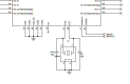
in both the boards we loaded DFU project to check BLE connectivity. in nRF52-DK, BLE function works great. but in our application board (nRF52832-CIAA) we cannot see the BLE advertising (32MHZ crystal is also not resonating)

please let us know what is the issue?? early response will be appriciated..

below attached the schematics.

image description

Parents
  • FormerMember
    0 FormerMember

    Did you remember to program the softdevice? What happens when you run the chip in debug mode, does it says that it's advertising?

    What is the load capacitance of the crystal. The value of the load capacitors should be approximately: C_27 = C26 = 2*C_l -4, C_l is the load capacitance of the crystal. The value of the load capacitors affect the frequency of the crystal, and hence, the transmit frequency.

    If the value of C_27 and C_26 is okay, could you upload the full schematic and layout? Both the schematic and layout is important when it comes to RF performance. If you want the schematic/layout to be kept secret, you can create a new support case from nordicsemi.com and refer to this thread.

    Update 04.11.2016: Generally, the RF-part of the schematic and layout should be a copy of the reference layout.

    Comments to the schematic:

    ANT pin: The components on the ANT pins should have the same values as the components in the reference layout. The purpose of those components is to filter harmonics. It means that R6 should be removed, and the value of L1 should be changed to 3.3 nH (nRF52832 CIAA).

    Antenna: The antenna will need a matching network, and as far as I can see, you are using a chip antenna, and the matching network should therefore be a pi-network. The pi-netowrk should be placed after L1.

    Comments to the layout: There is quite a lot of space on your board, I would think that it would be easier to use the QFN version?

    C5 and L1 (C3 and L1 in our reference layout): Should be placed exactly the same way as in the reference layout, with the same distance from the chip to L1 and from L1 to C5.

    Antenna: Which antenna do you use? Is it placed according to its reference layout? In order for the antenna to have the same characteristics as stated in the datasheet, our experience it has to be placed "exactly" the same way as in its reference layout.

    Traces/transmission lines: All traces/transmission lines in the RF part of the layout (between the ANT pin and the antenna) should be a 50 Ohm transmission line (coplanar waveguide). appCad can be used to calculate the appropriate width of the transmission line.

    Update 2, 04.11.2016: What happens when when you try to run the chip in debug mode? Can to "see" that it is running in main?

  • Hello Kristin,

    Yes, we programmed Soft device. we have not tested in debug mode.

    Load capacitance for crystal is 12pF. we varied the load capacitance from 8pF to 12pF, we couldn't see any results. we also tried replacing the Crystal on nRF52-DK with our application board crystal. it works fine.

    Other than loading softdevice and programming the BLE application code. do we need to load any other configuration settings?

    Also i will upload SCH and layout files. please review and let us know your feedback.

Reply
  • Hello Kristin,

    Yes, we programmed Soft device. we have not tested in debug mode.

    Load capacitance for crystal is 12pF. we varied the load capacitance from 8pF to 12pF, we couldn't see any results. we also tried replacing the Crystal on nRF52-DK with our application board crystal. it works fine.

    Other than loading softdevice and programming the BLE application code. do we need to load any other configuration settings?

    Also i will upload SCH and layout files. please review and let us know your feedback.

Children
No Data
Related