This post is older than 2 years and might not be relevant anymore
More Info: Consider searching for newer posts

nRF8001 Antenna design - Suggested layout

Hi,

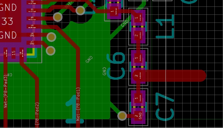
I am creating the first prototype for my BLE product and for now I used the suggested layout from the datasheet, but I am kind suspicious of that layout it seems very small (3,85 x 0,75 mm). I am using the layout from 17.5 topic (I downloaded the gerber).

Below the image from my layout (C6 = 1,8pF and C7 = 1,2pF) : image description

P.S: I am 100% newbie in RF Antenna design.

Regards,

  • FormerMember
    0 FormerMember

    The RF part of the reference layout consists of the nRF8001 and the required matching network for matching the chip to 50 Ohm. In addition to the reference layout, an antenna and a matching network for the antenna is needed. This whitepaper explains how to design a 2.45 GHz PCB antenna.

    Some general rules regarding design guidelines, taken from this tutorial:

    Matching networks: In RF, things work differently than in "regular" electronics, due to high frequencies (and short wavelengths). One of the resulting effects is that the phase of a signal will vary along the transmissions lines, as opposed to low frequencies where the wavelengths >> transmission lines, and this effect can be disregarded. If the system (chip and antenna) is not matched, there will be reflections of the signal in the transmission line, resulting in loss. The system can be matched using a 50 Ohm reference point; matching the chip and the antenna to 50 Ohm.

    General rule: The RF part of the schematic and layout should be a copy of our reference design. It means that not only the component values, but also the geometry, relative placement of the components with respect to each other, and the lengths of the transmission lines should be the same as in our reference design. *RF part: everything between the ANT pins and the antenna.

    The sections "Ground plane" the above reference tutorial are also relevant for nRF8001.

  • Thanks! Regarding the matching network, a load impedance of 15 Ω + j88 Ω is recommended for maximum output, however the matching network, from the layout, is for 50 Ω load impedance. Is there any particular reason for that? Is this done only for simplicity/easiness? P.S: I am still a newbie in RF =D

  • FormerMember
    0 FormerMember in reply to FormerMember

    The matching network will transform the impedance from the ANT pins to 50 Ohm. The point after the matching network will be a 50 Ohm reference point. The antenna can then be matched to 50 Ohm and connected to the 50 Ohm reference point without any loss due to impedance mismatch in the transmission line.

Related