This post is older than 2 years and might not be relevant anymore
More Info: Consider searching for newer posts

P0.11 connected to GND in the nRF52 reference PCB

image description
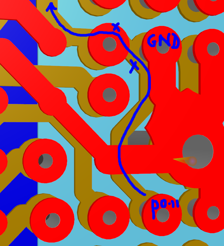
I notice that the track which runs from P0.11 (E4) is connected to GND at pads C3 and C4. Is this intentional? If P0.11 is required for GPIO usage, is it necessary to go to a 6 layer design? P0.11 is not connected to GND in the corresponding schematic...

Parents
  • Don't know which of the reference layouts you are looking at nor which tool you're using to look at them. I just looked at all three I think are current, normal, DC/DC and NFC and, on my gerber viewer there is no such connection, the P0.11 trace meanders correctly away on layer 1 and emerges untouched. My viewer doesn't show a via where you have 'GND' marked on your diagram.

    If there was it would be an error since it's not connected on the schematic.

    I got the reference layouts from the infocenter off infocenter.nordicsemi.com/.../nRF52832-CIAA_Ref_Layout_v1.0.zip that link.

    You can definitely do this on a 4-layer board, it's not even that tight.

Reply
  • Don't know which of the reference layouts you are looking at nor which tool you're using to look at them. I just looked at all three I think are current, normal, DC/DC and NFC and, on my gerber viewer there is no such connection, the P0.11 trace meanders correctly away on layer 1 and emerges untouched. My viewer doesn't show a via where you have 'GND' marked on your diagram.

    If there was it would be an error since it's not connected on the schematic.

    I got the reference layouts from the infocenter off infocenter.nordicsemi.com/.../nRF52832-CIAA_Ref_Layout_v1.0.zip that link.

    You can definitely do this on a 4-layer board, it's not even that tight.

Children
Related