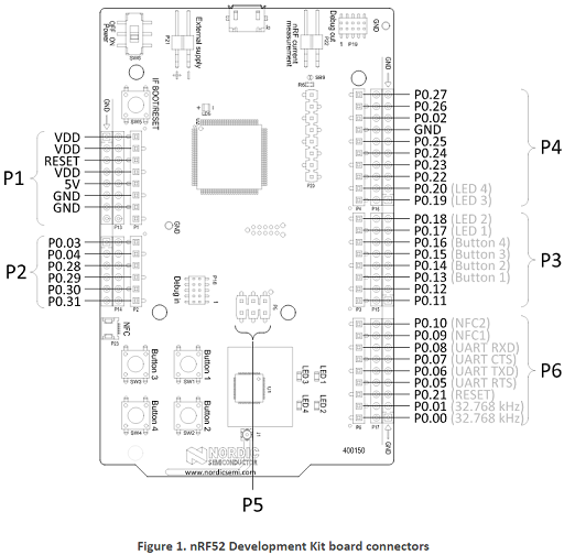
Hi, I'm using a nRF52 dk board as a switch to control a circuit. The problem is I not sure which gpio can be used to act as a switch to control the circuit. Thanks.
Hi,
You can see a list of all the GPIOs on the nRF52832 here. On the nRF52832 Development Kit some of the GPIOs are occoupied.
The buttons and LEDs uses the GPIOs from P0.13 to P0.20.
The 32.768 kHz crystal uses P0.00 and P0.01.
If you enable the NRF_LOG function in the SDK, P0.05->P0.08 is by default used for printing the data over UART.
P0.21 is used as a reset if the CONFIG_GPIO_AS_PINRESET
define is present.
If you use the NFC, the GPIOs P0.10 and P0.09 will be used by the NFC antenna.
The above bulletpoints are illustrated in this drawing:
If you really need to use the GPIOs used by the buttons, LEDs or the external crystal for something else, this can be done by shorting/cutting the solderbridges. All the other GPIOs are free to be used.
Thanks bro help a lot
P2/P8 Analog in
PIN #
Signal Name
NRF52832 Functions
1 A0 P0.03 / AIN1
2 A1 P0.04 / AIN2
3 A2 P0.28 / AIN4
4 A3 P0.29 / AIN5
5 A4 P0.30 / AIN6
6 A5 P0.31 / AIN7
P3/P9 Digital I/O
PIN #
Signal Name
NRF52832 Functions
1 D0 (RX) P0.11
2 D1 (TX) P0.12
3 D2 P0.13
4 D3 P0.14 / TRACEDATA[3]
5 D4 P0.15 / TRACEDATA[2]
6 D5 P0.16 / TRACEDATA[1]
7 D6 P0.17
8 D7 P0.18 / TRACEDATA[3] / SWO
P4/P10 Digital I/O
PIN #
Signal Name
NRF52832 Functions
1 D8 P0.19
2 D9 P0.20 / TRACECLK
3 D10 (SS) P0.22
4 D11 (MOSI) P0.23
5 D12 (MISO) P0.24
6 D13 (SCK) P0.25
7 GND N/A
8 AREF P0.02 / AIN0
9 SDA P0.26
10 SCL P0.27