Hey,
Could you please explain, in your reference designs, why you suggest to use solder mask clearances that cannot be produced?
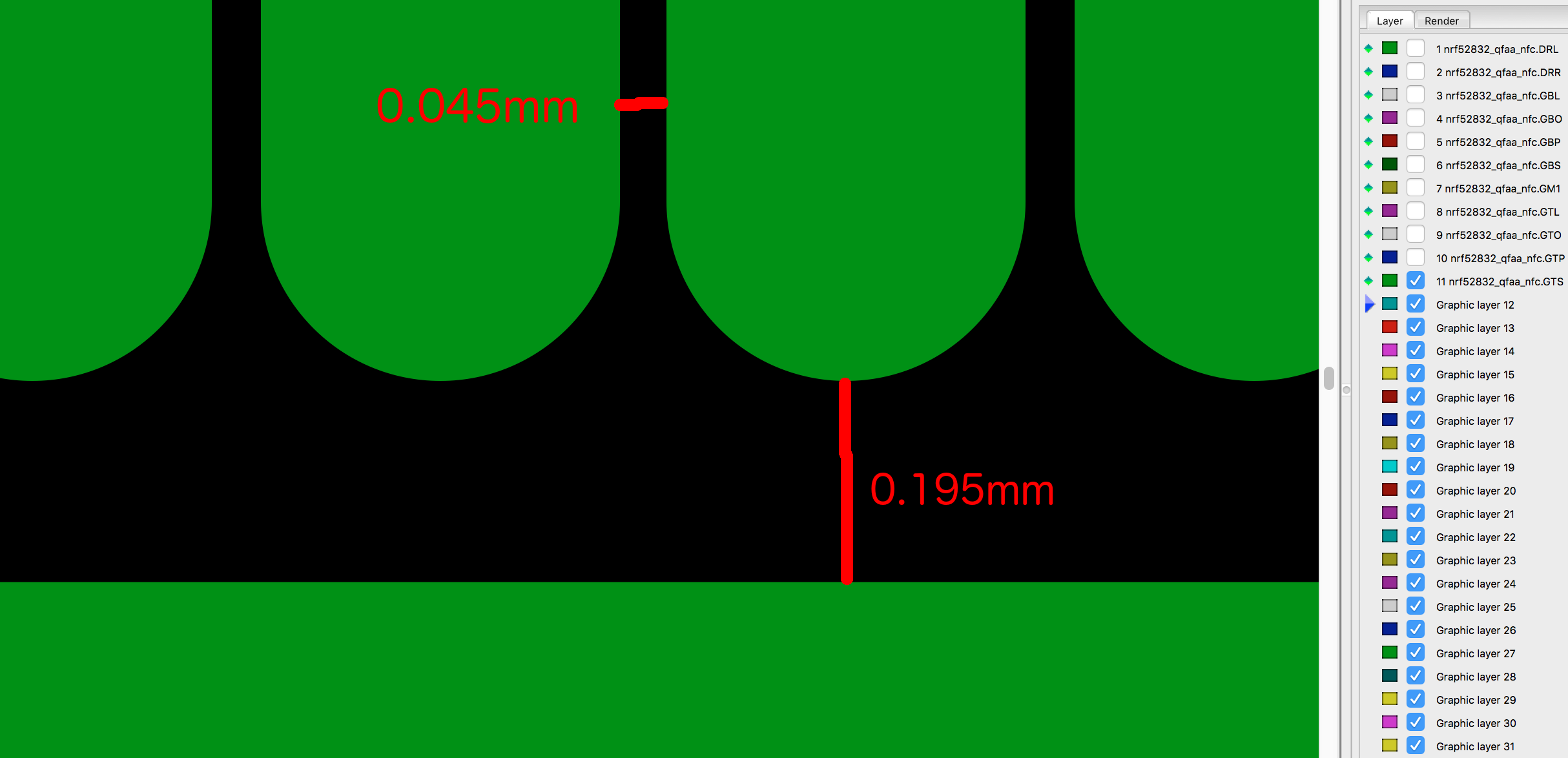
0.045mm is not possible produce and sometimes even 0.195mm is too thin line width to produce successfully. Many factories recommend only >10mil (0.254mm) solder mask line widths to be used.
An important question: If this is the case, what would be your recommended footprint layout for QFN48?
Because your reference design says the pins 31 and 45 has to be connected to directly bottom pad, non-soldermask defined bottom pad layout can lead to problems. Solder paste applied to pads of these 2 pins will "vanish" and can lead to poor connection. What is your suggested fix for this?
nRF52832 QFAx Reference Layout 1.1 solder mask layer:
What about, on paste layer, why you suggest to use 100% fill and no cross-hatching? There is a high probability this will lead to severe and expensive problems. During our production, we have noticed that even ~65% fill (cross-hatched, 5mil stencil) was too much of paste for nRF52832.
nRF52832 QFAx Reference Layout 1.1 paste layer (blue):

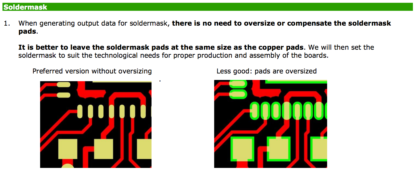
Common guidelines:

I am aware some factories suggest designers not to add any clearance but many times this is not the case. Often they prefer to follow the design files 1:1.