
Hi,
I am using BMD300 to develop my projects. I am working on SAADC sample example in SDK12.0.0. I am sampling the SAADC at a rate og 1000 sps. following is the saadc_ini() function:
    void saadc_init(void)
{
    ret_code_t err_code;

   //###########################################ANI0
    nrf_saadc_channel_config_t channel_0_config;
    channel_0_config.resistor_p = NRF_SAADC_RESISTOR_DISABLED;
    channel_0_config.resistor_n = NRF_SAADC_RESISTOR_DISABLED;
    channel_0_config.gain       = NRF_SAADC_GAIN1_6;
    channel_0_config.reference  = NRF_SAADC_REFERENCE_VDD4;
    channel_0_config.acq_time   = NRF_SAADC_ACQTIME_10US;
    channel_0_config.mode       = NRF_SAADC_MODE_SINGLE_ENDED;
    channel_0_config.pin_p      = NRF_SAADC_INPUT_AIN0;
    channel_0_config.pin_n      = NRF_SAADC_INPUT_DISABLED;

    nrf_drv_saadc_config_t saadc_config;

    //Configure SAADC
    saadc_config.resolution = NRF_SAADC_RESOLUTION_12BIT;                                 //Set SAADC resolution to 12-bit. This will make the SAADC output values from 0 (when input voltage is 0V) to 2^12=2048 (when input voltage is 3.6V for channel gain setting of 1/6).
    saadc_config.oversample = NRF_SAADC_OVERSAMPLE_DISABLED;                              //Set oversample to 4x. This will make the SAADC output a single averaged value when the SAMPLE task is triggered 4 times.
    saadc_config.interrupt_priority = APP_IRQ_PRIORITY_LOW;


    err_code = nrf_drv_saadc_init(&saadc_config, saadc_callback);
    APP_ERROR_CHECK(err_code);

    err_code = nrf_drv_saadc_channel_init(0, &channel_0_config);
    APP_ERROR_CHECK(err_code);

    err_code = nrf_drv_saadc_buffer_convert(m_buffer_pool[0], SAMPLES_IN_BUFFER);
    APP_ERROR_CHECK(err_code);

    err_code = nrf_drv_saadc_buffer_convert(m_buffer_pool[1], SAMPLES_IN_BUFFER);
    APP_ERROR_CHECK(err_code);

}
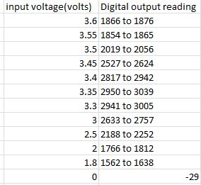
When I am giving variable analog input voltage , I am not getting the expected Digital output. Following table shows the analog inputs and corresponding digital values:
Following are my concerns:
-
Is it displaying 2's compliment values? and if yes for 12 bit resolution values should lie between -2048 to 2047. So if I am not wrong maximum output should be equal to 2047 and which is equal to reference of SAADC. So why the values are not in the range?
-
If it is not 2's complement values should lie in range 0 to 4095. But SAADC values seems to decrease after I apply voltage more than 3.4 volts. Why is it so?
-
what is the reference. Is it VDD or VDD/4(mentioned in the documentation)?
-
does the calibration required as it consumes more time.(which may affect my operation)
I know it is somewhat lengthy question or someone might have asked previously. But I couldn't find the proper solution. So If someone had worked over it previously please make understand these things..
Thanks in advance!!
