This post is older than 2 years and might not be relevant anymore
More Info: Consider searching for newer posts

Problem with radio frequency custom board. Balun mismatch?

Hi Nordic,

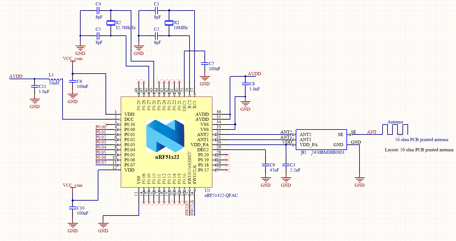
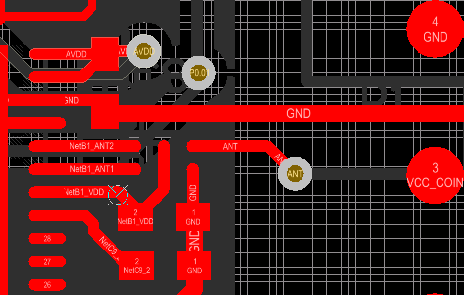
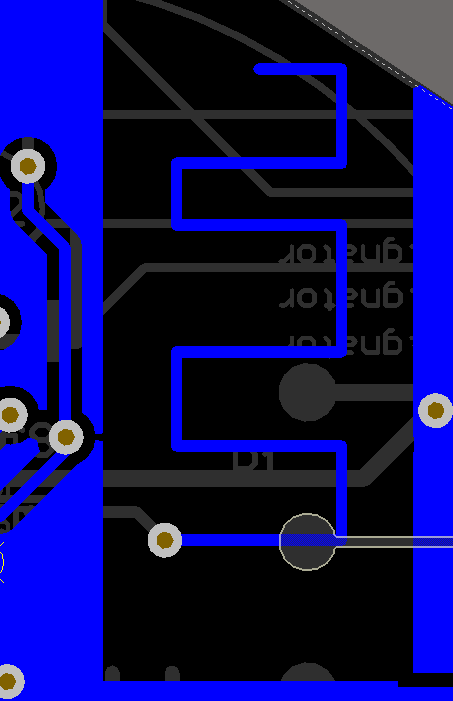
I have an application that perfectly runs in the nrf51DK but that does not work in my custom board. In my custom board everything else works (i2c, leds lighting, etc..) except for the communication related stuff. I think I am having some problems with the antenna. The balun I am using is 2450BM08B0003, which is the one recommended in this page for the nrf51422. As a detail, the components in the board have been placed by hand and soldered with oven reflow.

Here I attach the parts of the design that have to do with the communication.

image description

image description

image description

Any idea on how to debug my problem? I have no idea what is going on. I have been reading some other people have the exact same problem, but I have yet no idea of a proper solution.

PS: Sometimes we can transmit data from our custom board to the nordic developer kit. But not the other way around, we cannot receive data. Is this usual?

Thanks for your help!

Parents
  • Also are those traces (gray lines) underneath your antenna? Another thing you would need to check to the impedance from the feedline to the balun and then the balun to chip. determine the transmission line impedance of ANT, ANT1 and ANT2. Those could be causing your mismatch as well.

    If you have access to an network analyzer let me know. Problem is easy to resolve with one of those.

  • Traces underneath the rf antenna is a bad practice. The antenna will not be able to properly radiate. If you look at the dk you will notice it has a keep out zone around the antenna. If you were able to get a hold of a network analyzer you would basically perform a S11 measurement on the antenna. You would want to make sure you have good return loss -9 or higher in the freq range of bluetooth. 2.4-2.45ghz. I normally use the following markers; 2.4, 2.44 & 2.45 ghz.

    Since you have traces under the antenna my recommendation would be to following. Redo the pcb with no traces around or under the antenna. You need a keep out zone. I would also place a pi network or some lumped configuration between the antenna or the balun to aid in matching.

    For these boards you could cut the antenna and place a sma on top layer and use an external antenna for now.

    Oh also try to avoid vias in the antenna path. With the proper keep out you should have no need to change layers.

Reply
  • Traces underneath the rf antenna is a bad practice. The antenna will not be able to properly radiate. If you look at the dk you will notice it has a keep out zone around the antenna. If you were able to get a hold of a network analyzer you would basically perform a S11 measurement on the antenna. You would want to make sure you have good return loss -9 or higher in the freq range of bluetooth. 2.4-2.45ghz. I normally use the following markers; 2.4, 2.44 & 2.45 ghz.

    Since you have traces under the antenna my recommendation would be to following. Redo the pcb with no traces around or under the antenna. You need a keep out zone. I would also place a pi network or some lumped configuration between the antenna or the balun to aid in matching.

    For these boards you could cut the antenna and place a sma on top layer and use an external antenna for now.

    Oh also try to avoid vias in the antenna path. With the proper keep out you should have no need to change layers.

Children
No Data
Related