This post is older than 2 years and might not be relevant anymore
More Info: Consider searching for newer posts

NRF51822 PCB layout review

Hello,

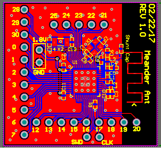
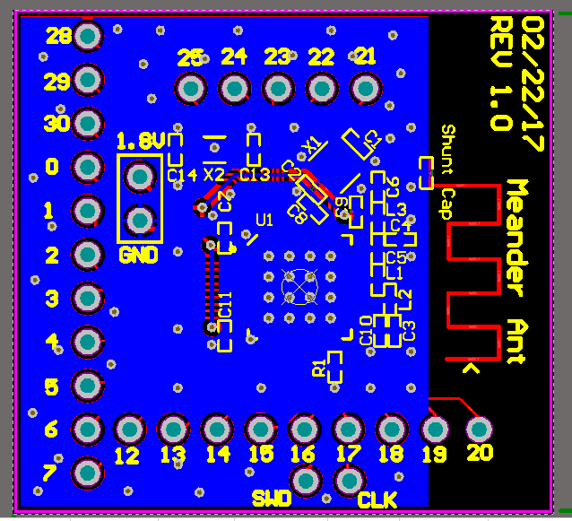
I recently finished up the NRF51822 pcb board that I plan on getting printed. I used the reference design file provided by Nordic (NRF51x22_qfax) but added the following things:

  • Meander Antenna taken from NRF51-Dongle with a bit more length added for adjustment
  • Shunt Capacitor for the Meander Antenna
  • Through-holes connected to most of the I/O pinouts from the chip for breakout
  • Through-holes for power in (1.8V & GND)
  • Increase in GND plate size with vias to match

I am rather new at working with the NRF51 series as well as PCB design. Any advice would be great help. I am mostly concerned over the way my antenna is structured and if a single shunt cap should be enough for this.

Thanks!

Image of Front

Image of Back

Altium PcbDoc Source File

Parents
  • I just took a look at the jpeg's you sent out and not the Altium file. It looks like you are making a development styled board.

    I would suggest you implement both the dc/dc for up to 3.6vdc and a 1.8 vdc low voltage connection. It seems like more people are likely to run it on 3.3 from other sources than a 1.8vdc source. This way they could do either.

    The balun/matching for your meander is kind of messy. There are several good chip style LC baluns with match and harmonic filtering for the 51822. They will take up less board space and give you an easier RF solution. One is made by Johanson.

    You should put more capacitance local to the 51822. It looks like you are using the bare minimum from the reference design and you may have lost some of the bypass caps. Processors need quite a bit of instantaneous current to operate and local caps provide this. Also, if the device is run on a coin cell these have very high internal resistance and the losses could put you locally into a brown out state during a Tx burst.

    The footprint for the 51822 seems ok, but I didn't measure it. Looks like a nice via grid.

    You broke the ground plane to run power from the left side to the right side. The clock lines will radiate more this way and you will probably introduce some clock noise and harmonics into the nearby gpio/adc connections. At least you did this at right angles, but it could give you some headaches.

    Connections 19 and 20 are kind of in the middle of nowhere and will couple a little with the meander. If it was me, I would figure out a way to move the connections around so they are all back behind the ground plane.

    If it's meant to be a development board that someone may permanently mount inside a product, you should put some unplated mounting holes on the board. This will make mounting a lot easier than drilling holes.

  • I am not sure which extra converter you are referring to. The 51822 has an on chip buck converter that only requires an external cap and inductor. The only thing you need to do is supply the 51822 with 3.0 -3.3 and let the the 51822 do it's job. This will give you gpio at the higher vdd (3.0-3.3) which will likely help out with gpio communications with other devices. The soft device automatically controls the on chip converter and only brings it up when necessary. You could probably even make a case for running it at 2.7v. This would give you a little more operating range on the lithium battery. You just need to run all your peripherals at that same voltage what ever you choose. In case I didn't make that clear earlier, if you choose 1.8 you need to run all your peripherals at 1.8, similarly if you choose 3.0 you need to run all the peripherals at 3.0.

Reply
  • I am not sure which extra converter you are referring to. The 51822 has an on chip buck converter that only requires an external cap and inductor. The only thing you need to do is supply the 51822 with 3.0 -3.3 and let the the 51822 do it's job. This will give you gpio at the higher vdd (3.0-3.3) which will likely help out with gpio communications with other devices. The soft device automatically controls the on chip converter and only brings it up when necessary. You could probably even make a case for running it at 2.7v. This would give you a little more operating range on the lithium battery. You just need to run all your peripherals at that same voltage what ever you choose. In case I didn't make that clear earlier, if you choose 1.8 you need to run all your peripherals at 1.8, similarly if you choose 3.0 you need to run all the peripherals at 3.0.

Children
No Data
Related