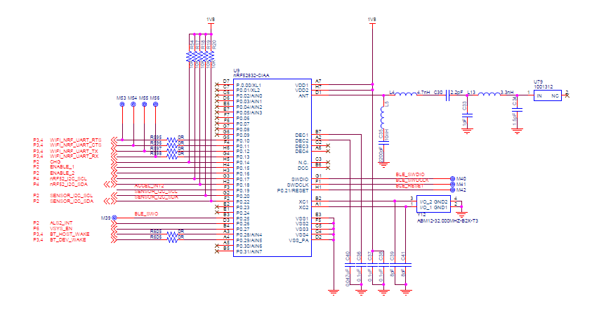
The general rule for a schematic is that it should be a copy of our reference schematic. It means that on the ANT pin, there should be a LC-filter, C = 1.0 pF and L = 3.3 nH. In addition, a matching network for the antenna is needed, in your case it's a pi-filter and it consists of C33, L13, and C34.
I would recommend you to go through the shcematic and make sure that it is a copy of the reference schematic. The reference layout and schematic can be found here.
It can also be useful to have a look at this tutorial (General PCB design guidelines for nRF52).
Thank you so much for the feedback, I implemented the matching circuit according to the reference design, since this is a DEV BOARD that I am building, I am planning to use a SMA connecter O/P. The PCB guidelines page was useful. Much appreciated for your help.
Thank you so much for the feedback, I implemented the matching circuit according to the reference design, since this is a DEV BOARD that I am building, I am planning to use a SMA connecter O/P. The PCB guidelines page was useful. Much appreciated for your help.