
We would like to review the following impedance matching circuit:
We would like to review the following impedance matching circuit:
Just curious. What Cad package you are using ?
Also.
I asked a similar question, though for the nRF52840 directly on the MyPage support, but Nordic require Gerbers or Altium files before they would review the schematic. i.e I don't think they can simply review a schematic on its own, and you would also need to include details of the part numbers of the components you intend to use for the antenna circuit etc
Hi Roger,
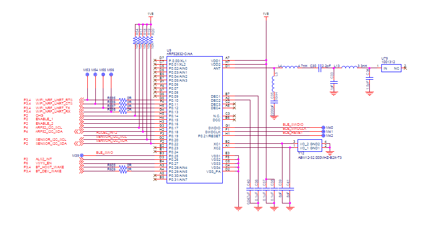
Thank you so much for the comment, I am using OrCAD and Allegra. The reason for posting this question is because, I have a space constraint and I am trying to remove L4, L5, C30 and C35. The traces are fairly thin and I would like to know if we can match and tune the circuit with L13, C33 and C34. The antenna I use is a chip antenna from ethertronics.
No worries
I think you best option is to register on Noric's MyPage support system
www.nordicsemi.com/.../register
And send this as a support request, including you gerber file for the PCB (as I don't think they accept anything other than Altium files)
I'm now using KiCad, because the cost of Altium is prohibitive on niche products. (Previously I'd been using Eagle)
BTW. I was a bit surprised about the way you designed your schematic symbol for the nRF52832, as it doesn't look anything like the schematic symbol that Nordic have published
I know the schematic symbol does not need to look anything like the physical footprint, but as component placement is critical on these devices, I suspect that Nordic made the schematic and physical representation virtually the same to help with the translation of the schematic to the PCB design.

The general rule for a schematic is that it should be a copy of our reference schematic. It means that on the ANT pin, there should be a LC-filter, C = 1.0 pF and L = 3.3 nH. In addition, a matching network for the antenna is needed, in your case it's a pi-filter and it consists of C33, L13, and C34.
I would recommend you to go through the shcematic and make sure that it is a copy of the reference schematic. The reference layout and schematic can be found here.
It can also be useful to have a look at this tutorial (General PCB design guidelines for nRF52).
Hi Kristin,
Thank you so much for the feedback, I implemented the matching circuit according to the reference design, since this is a DEV BOARD that I am building, I am planning to use a SMA connecter O/P. The PCB guidelines page was useful. Much appreciated for your help.
