
Hi,
See attached photo for layout placement of the trace antenna.
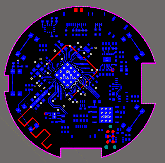
Altium PCB File: 108-0013-01 PCBA MAIN.PcbDoc
Background:
This is a design for a wearable watch style product. Tight design mechanically, and hard to find an ideal placement for the antenna. There are 3 switches on the left side of the PCB, 2 switches and a USB connector on the right, two large FPCs for the display at the top, and a vibration motor in the cutout on the bottom.
A first pass at component placement has been completed, traces have not been completed. The layout design is based off a hybrid of the 'nRF52840 Preview Development Kit - Hardware files 0_9_0' and 'nRF52840-QIAA Reference Layout 0_5' (the 'var5' project), as well as the old nRF51 dongle for the meandering antenna.
The SMA connector recommended in the Nordic designs is placed (and shorted) for testing/tuning only (trace will be cut when using it). It will be DNP in production.
Questions:
-
I would expect the added trace by placing a series SMA connector would affect RF performance. How do you recommend to account for this? Is the effect as simple as adding the length from the added trace that shorts the SMA conector to the length of the antenna when optimizing it for quarter wavelength? Is the shunt capacitor enough?
-
There is a concern for placement of the antenna right below the switch (MPN: TL1014). Sounds like there shouldn't be an issue placing the antenna on the other side of the PCB through a via. For the wearable device we don't need the full range of BTLE. Most use cases will be a user syncing to their phone while wearing the watch. Should we expect reasonable performance given our use case?
