This post is older than 2 years and might not be relevant anymore
More Info: Consider searching for newer posts

nRF52832 ANT pin Impedance

Hi Nordic Forum!

We're currently tuning our antenna since we runed with some problems during our EMC testing.

In that regard, what is the impedance (both input and output) of the antenna pin (pin 30), when used for Bluetooth?

I know that for the nRF51 series it was 15 + j85 (Between ANT1 and ANT2), but I don't think that holds for the nRF52 series.

Thanks in advance

Parents Reply Children
  • This is somewhat confusing for me.

    1. Isn't this package dependent?
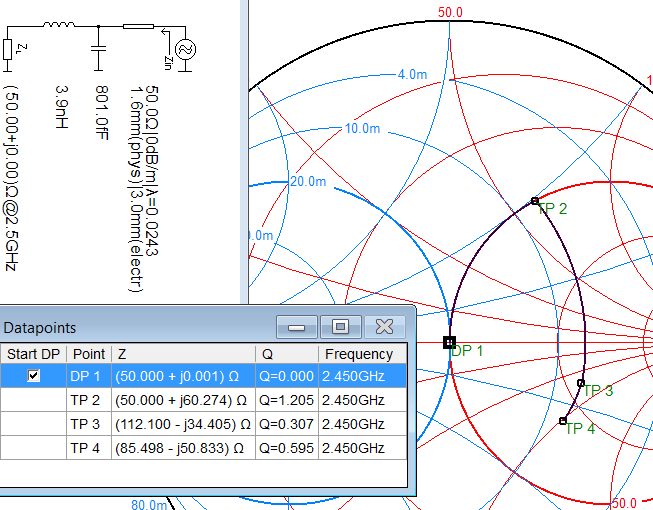
    2. In the reference design (let's take the nRF52832CIAA as example) the matching components are L = 3.3nH and C = 1pF

    Assuming that these components result in 50Ohm I calculated the impedance of the pin and got 78 + j48 Ohms. The reason why this bothers me is that I'd like to match the nRF and the antenna with one single PI-filter and not with the proposed LC and an additional PI-filter due to size limitation constraints.

  • There are a few questions here so:

    1. Yes antenna port impedance is package dependent. You will notice on the spec the recommended load is a little different for the WLCSP vs. QFN versions.

    2. No you can't calculate it like that. For starters your calculation doesn't include the effects of the vias, component to component spacing, it should use real not idealized component physics and also it assumes a 50 ohm strip going into the WLCSP. The designs always have a parasitic inductance going into the chip due to the pin pitch.

    Also, you can't assume the recommended antenna load results in a 50 ohm match.  Power amplifiers rarely perform optimally in a conjugate match condition. Mis-match is often included to optimize the IP3 and harmonic performance.

    On your custom board, your only course of action is to come up with a match that optimally conveys power to your antenna, while maximizing IP3 performance and minimizing harmonic output.

  • Is there actually a recommended load somewhere in the spec? 

    If so, I can't find it.  I know that different matching networks are given to get to 50 ohms but to the point about non-ideal components and board parasitics, these are not really transferable to another board design.

  • If the Load impedance of antenna pin should be 53 + j66 Ohms then the ANT pin impedance should be conjugate of the same 53 - j66 Ohms right?

    This will help us instead of keeping the load as 53 + j66ohms, we will do matching from pin impedance 53 - j66 Ohms to final antenna impedance with matching circuits.

    Please confirm, Because our antenna impedance is not 50Ohms.

Related