
We are currently designing a prototype board for our product using the nRF52832. We need to calculate the transmission line with on a 4 layer PCB. The stack-up looks like this:
Copper 1 35 um - Signal (with surrounding GND)

Dielectric 1-2 0.175 mm (e.g. 1x Prepreg 7628 AT05 47% Resin) TG130 dielectric constant 4.29

Copper 2 35 um - GND

Dielectric 2-3 1.13 mm (6x 7628M 43% Resin) TG150 dielectric constant 3.96

Copper 3 35 um - VCC

Dielectric 3-4 0.175 mm (e.g. 1x Prepreg 7628 AT05 47% Resin) TG130 dielectric constant 4.29

Copper 4 35 um - Signal (with surrounding GND)
As per your suggestion, we put a keep-out on the two inner layers of the PCB. There are 2 things we are not entirely sure about:
Given this PCB calculator:
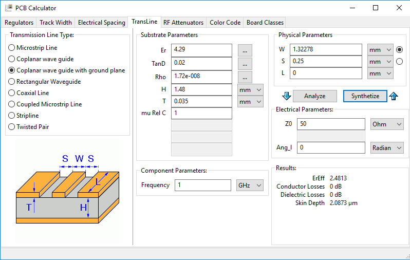
- Since we have a keep-out on both inner layers, should H be the distance between the top layer and the bottom layer?
- If 1 is true, what is the dielectric constant (Er)? (because the constant is different between the top - second layer pair and the second-third)
