This post is older than 2 years and might not be relevant anymore
More Info: Consider searching for newer posts

Cannot find my Device on nRF connect

image description image description image description

hello friends:) i have some problem during making my products, it's an a interface board with ble that generates UART signal for other board

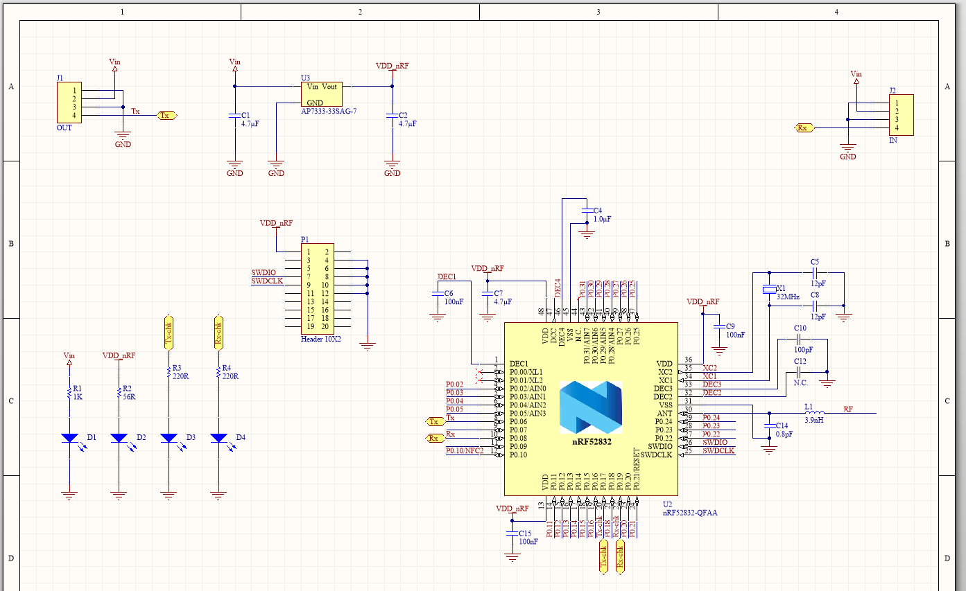
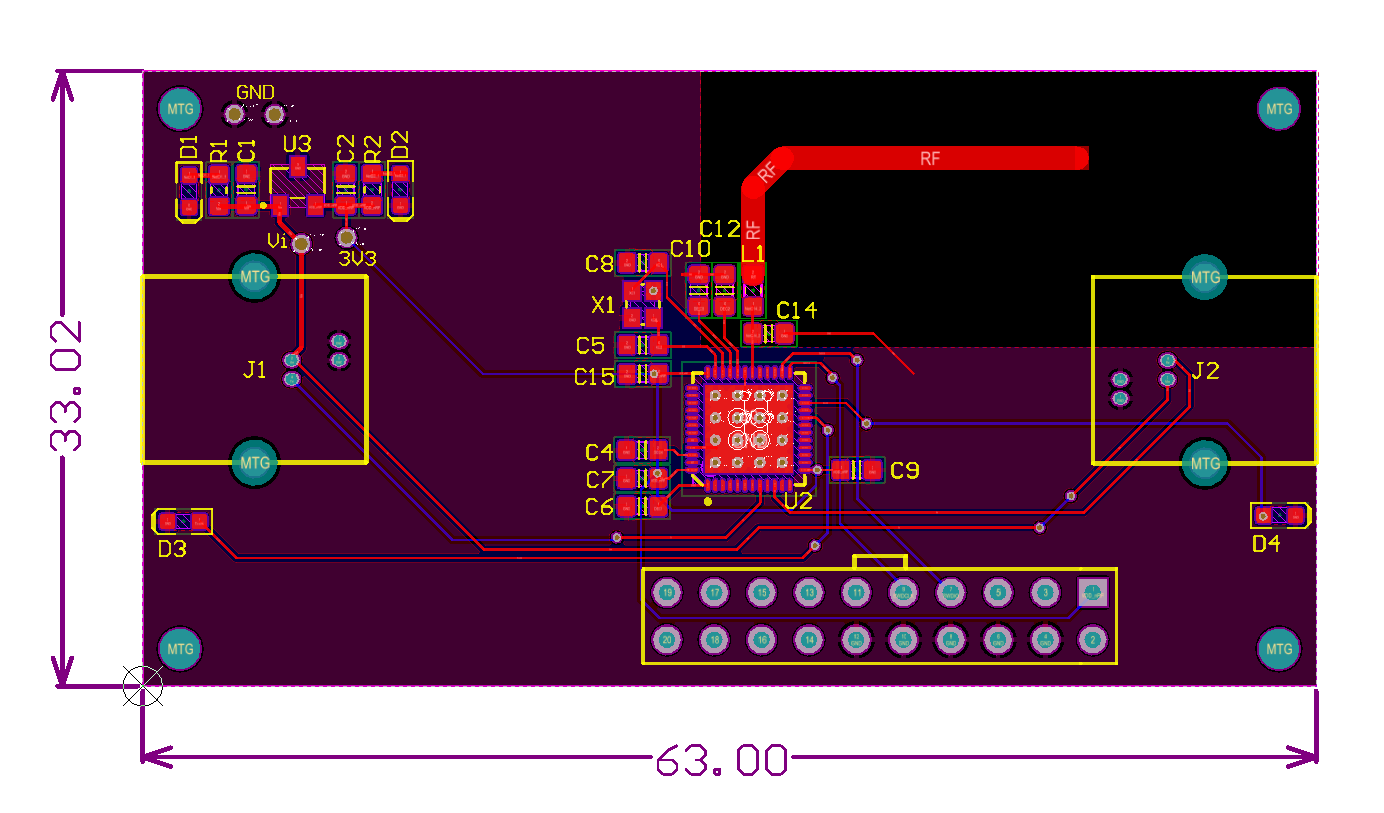
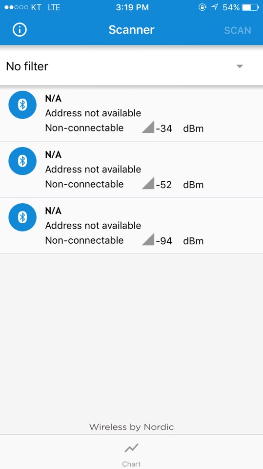
and i made an schematic with reference design and i got my pcb and assembled it, but like picture 3; maybe -34dbm is my board, it can't load any informaion about it; chip is working that i checked with blinky application

someone says the antenna is problem... but i have no idea that what is a problem.. it really makes me mad.. pls someone help me....

Parents
  • Hello Nomyar

    There are a few deviations in your design and layout, which can cause problems. First you have not included the matching capacitor for the PCB trace antenna, see this blogpost. The capacitor C14, and inductor L1 are there to match the chip to 50 Ohm, however an additional shunt capacitor should be located close to the antenna feed-point. This shunt capacitor, along with the antenna length and width, will ensure the antenna is matched to 50 Ohms.

    In the layout, you should have a ground plane, orthogonal on the feed-point of the antenna, stretching a minimum of a quarter of a wavelength in each direction (though preferably much more, especially when the antenna trace is bent). It is important that this ground plane is unbroken, and no other trace-lines or components are placed within the keep-out zone of the antenna. In your layout the inductor L1, the capacitors C10, C12 and C14 and the trace-line from capacitor C14 are all within the antenna keep-out zone. You also have a ground plane quite close to the antenna on the left side.

    These things can affect the antenna impedance, and radiation pattern.

    The components in the matching network (C14, L1 and the antenna shunt capacitor) as well as all trace-lines leading from the chip to the antenna must have a solid ground plane underneath, on the bottom layer of the PCB. This ground plane should be as large, and unbroken, as possible. However, make sure not to put a ground plane underneath the antenna. No ground plane should be within the antenna keep-out zone.

    I recommend you read both the blogpost I linked to in the beginning of my answer, it contains links to antenna design guides as well. Also be sure to read the PCB guidelines in the nRF52832 product specification.

    I also recommend you look at, and as far as you can copy, the layout of the nRF52832 development kit. You can find the hardware files here

    Best regards

    Jørn Frøysa

  • I think the cause of the problem is a combination of things. Antenna matching could be one, the fact that there is no ground plane under the transmission lines and components leading out to the antenna is another large factor.

Reply Children
No Data
Related