This post is older than 2 years and might not be relevant anymore
More Info: Consider searching for newer posts
This discussion has been locked.
You can no longer post new replies to this discussion. If you have a question you can start a new discussion

Can not find the device

Hi,

I am working on a custom design for NRF52832. The schematic and pcb layout are as follows. However, it seems that I can not get the signal working correctly. Would you please take a look and give me some tips/advices/suggestions? Thank you very much.

The custom board is just for a small keyboard which is space limited. For testing, I am using pcb antenna only. I soldered 2 boards and both of them have the same problem:

  1. Use SWD to burn softdevice and hrs sample(removed the external LFCLKSRC and turned on RTT logging)

  2. It doesn't show in nRF connect/toolbox

  3. I tried other samples like hid_keyboard, still the same problem: It doesn't show in nRF connect/toolbox/iOS/android.

  4. No any errors prompt in RTT logger.

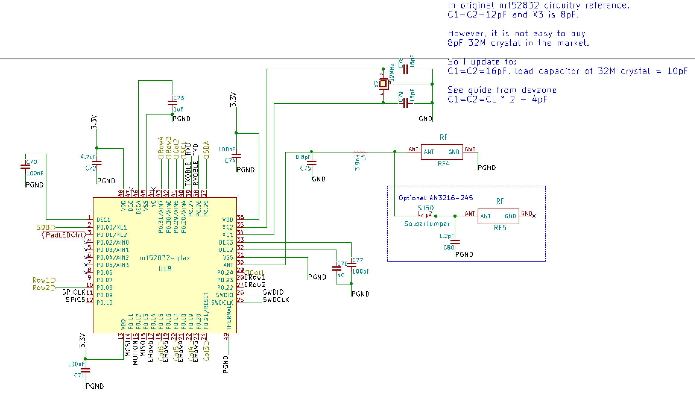
I suspect this is a pcb antenna design issue. However, by reading a lot from infocenter, still I can not find what the problem is. Should I solder a shunt capacitor in C76?

According to the guideline here: devzone.nordicsemi.com/.../ I am using:

  1. X7 = 32M crystal, load cap = 10pF

  2. C79=C78 = 16pF

  3. nRF52832-QFAA, 2 layers, 1.6mm thickness, and FR-4 dielectric.

  4. To avoid side effects, all other components like LEDs are not soldered in my testing boards.

image description

image description 
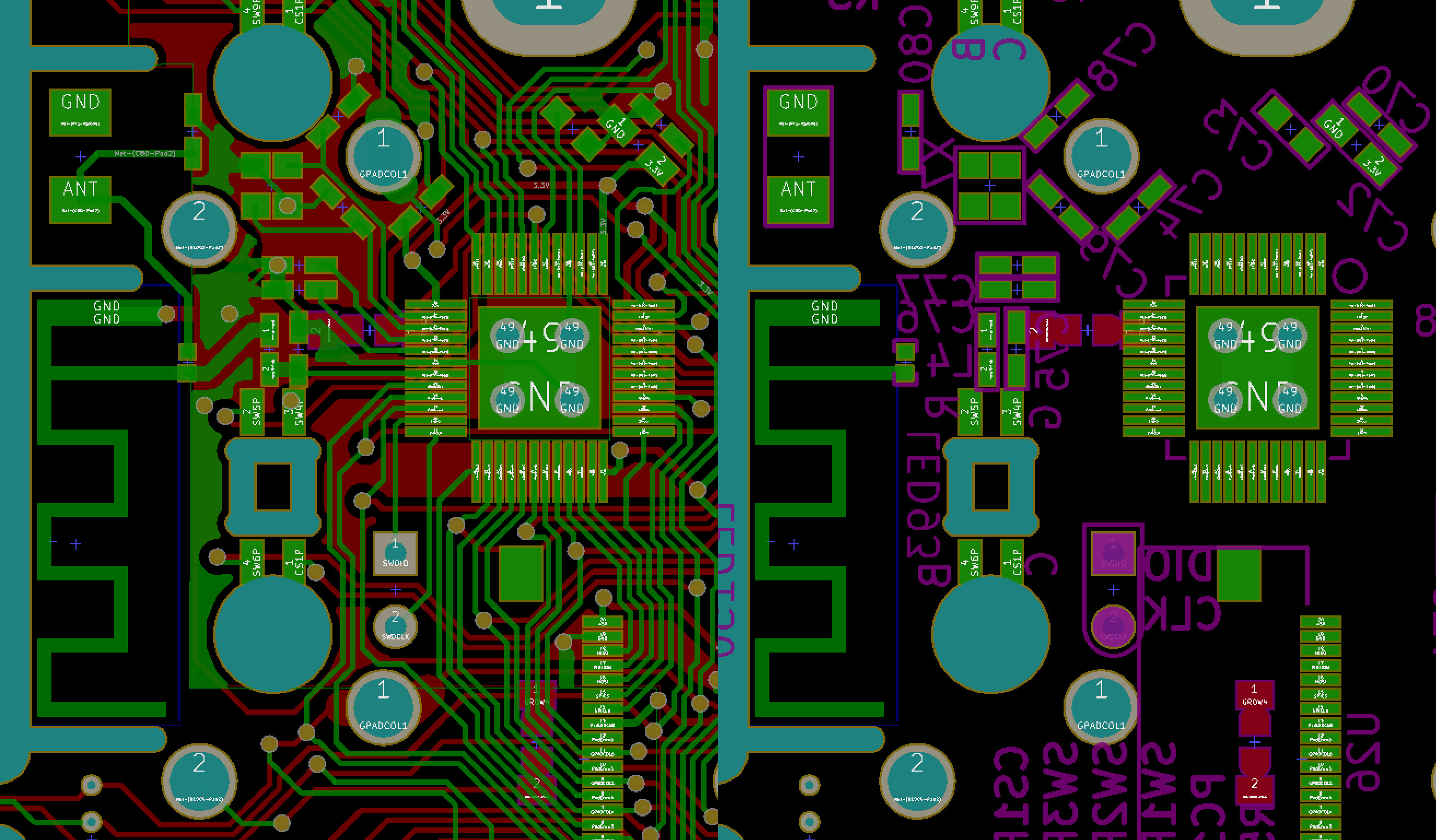
(Left side is Back copper layer and right side is the Silk layer)

My Dev environment: Windows 10, Jlink 5.12f, SDK 13.0.0. Please let me know if you need further information. Thanks very much.

Yours sincerely,

Vincent

Parents
  • The chip antenna isn't going to help out your problem. Your layout for the chip antenna is poor compared to the F hybrid. If the nRF is working you should be able to pick it at close range.

    On the load caps, what I meant is that I believe 16pF is the wrong value. I reviewed the Nordic guidance and it didn't address the parasitic capacitance of the circuit. This will change the load caps by a few pF.

    Do you not have just an oscilloscope to measure the frequency of the 32MHz with?

    If you go through a re-design, you have very significant problems with your ground plane. It is broken in most areas under the nRF. This alone could cause the nRF to be unstable and not transmit.

    Also, your schematic shows that you split the power and RF grounds. This is wrong for this device.

    Happy to continue helping. But you are going to need to do a little testing a provide a little more feedback.

Reply
  • The chip antenna isn't going to help out your problem. Your layout for the chip antenna is poor compared to the F hybrid. If the nRF is working you should be able to pick it at close range.

    On the load caps, what I meant is that I believe 16pF is the wrong value. I reviewed the Nordic guidance and it didn't address the parasitic capacitance of the circuit. This will change the load caps by a few pF.

    Do you not have just an oscilloscope to measure the frequency of the 32MHz with?

    If you go through a re-design, you have very significant problems with your ground plane. It is broken in most areas under the nRF. This alone could cause the nRF to be unstable and not transmit.

    Also, your schematic shows that you split the power and RF grounds. This is wrong for this device.

    Happy to continue helping. But you are going to need to do a little testing a provide a little more feedback.

Children
No Data
Related