
Hello,
I developed a Nordic board with 2450AT18B100 chipset antenna. I follow the design of Solar Powered Sensor Beacon.
infocenter.nordicsemi.com/index.jsp I test it and it works fine, but I want to tuning the antenna in order to get minimum return lose in signal.
So, I implement this antenna circuit in my board.
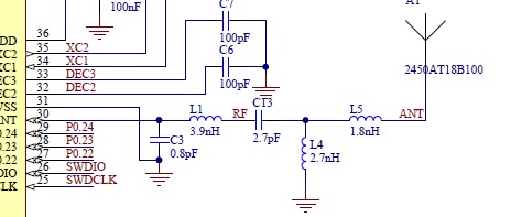
From johanson technology values are:
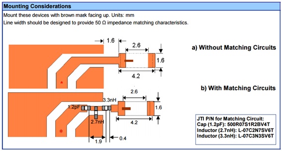
I suppose that from C3 and L1 you have to modify some references values of johanson chip antenna.
In general, my questions are:
Can you explain me each part of this circuit?.
Can you explain me why do you change this values and how do you calculated?.
Can you explain me how tuning the antenna?. Because your reference document for that do not explain how to do it in this case.
infocenter.nordicsemi.com/.../nwp_017.pdf
Thanks in advance.
Jose.
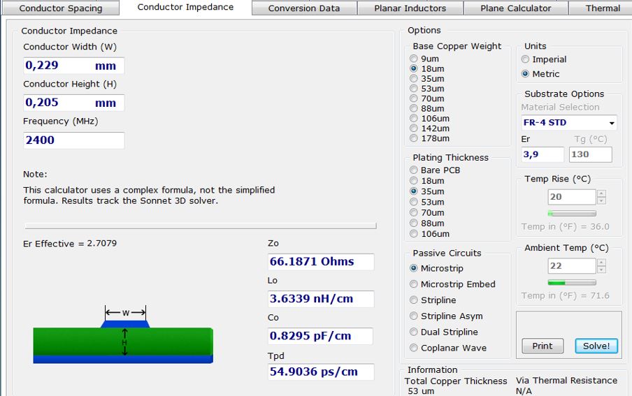
Others attached files. Conductor Impedance

Trace Lenght Solar Beacon
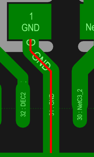

 Also I was checking the distance. In Solar Beacon board, the distance is 1.694mm and in “nRF52 matching network.pdf” document is 0.9mm, do you know why???. I suppose that you are taking other reference. You can see in the picture below my reference of 1.694mm because I think that GND is the thermal/ground PAD of the nRF52.