This post is older than 2 years and might not be relevant anymore
More Info: Consider searching for newer posts

NRF52832 BLE Trace Width

Hi I am trying to design a custom BLE board using NRF52832 by following the reference layout. I am new to RF design and I have got a few questions that I would really appreciate if someone could answer for me thanks.

To design the antenna and matching circuit I am following the layout of the Solar powered beacon which uses Johanson's 2450AT18B100 chip antenna. I am also using Johnson's filter 2450FM07A0029 to match the impedance of NFR52832. However the matching components used in the Solar powered beacon differs from 2450AT18B100's recommended values, is this a result of tuning? So would it be best for me not the solder any components then tune the circuit first with a network analyzer? Or could I just copy the reference design but same trace width,thickness, component spacing and pcb material buildup?

Also based on the parameters from the stack manager and trace width of 15mil the characteristic impedance using online calculators comes out to be 114 instead of 50 or does it not matter in this case due to how short the trace is (below wavelength of the BLE)?

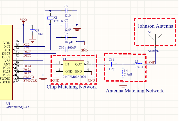
Here is my schematic: image description

Thanks for the help.

  • First, at 2.4GHz even a few mm of change in the distances between devices and components is significant. The matching components are fixing impedance problems. On a board the wave travels at less than the speed of light due to Er. For most FR4 boards about 64% of the speed of light. At 2.4GHz every 1.2mm of distance is 10 degrees of rotation around the smith chart. On a smith chart every 360 degree rotation corresponds to half a wavelength. If all these things were 50ohm they would just spin around the center of the smith chart. However, they are not and 10 or 20 degrees will change the apparent impedance matching problem considerably.

    The most likely reason your solar beacon example has different matching components is that the layout is a little different and someone took the time to rematch it. If you choose to use the example as is you will need to faithfully copy the design including trace widths, ground pours, trace lengths, ground pour setback from traces, component sizes, board materials and grounding vias. Only then can you be reasonably confident that it will work as it did before.

    However, as we often note on this blog, even when you painstakingly copy a design, rarely are the two the same and you should be prepared to do some re-matching work with a VNA.

    Assuming you used the correct stackup and constants for your waveguide model, the reason you got 114 ohms is that it is not necessary to use 50ohm traces to make an RF design. On very small boards it is often unrealistic to get a trace to 50ohm due to the widths required vs. the component sizes. Characterized traces only simplify some aspects of matching and also allow you to get accurate numbers on a 50 ohm port (such as SMA) but they are not required. You can actually do anything from choose a different impedance that is more similar to your loads and sources. Or, not normalize the sources and loads at all and just do conjugate matches throughout the design. The only real benefit a characterized trace provides is that when the source or load is the same impedance as the trace you know you can place the next device in the chain are far or as close as you wish and its impedance won't change. Only the signal level changes due to losses. But if the source or load impedance is not the same as the trace then the impedance will change considerably even after only a few mm's.

  • FYI: We'll (Nordic's Tech Support Department) review your schematics and gerber files free of charge if you submit them through our Mypage portal.

Related