
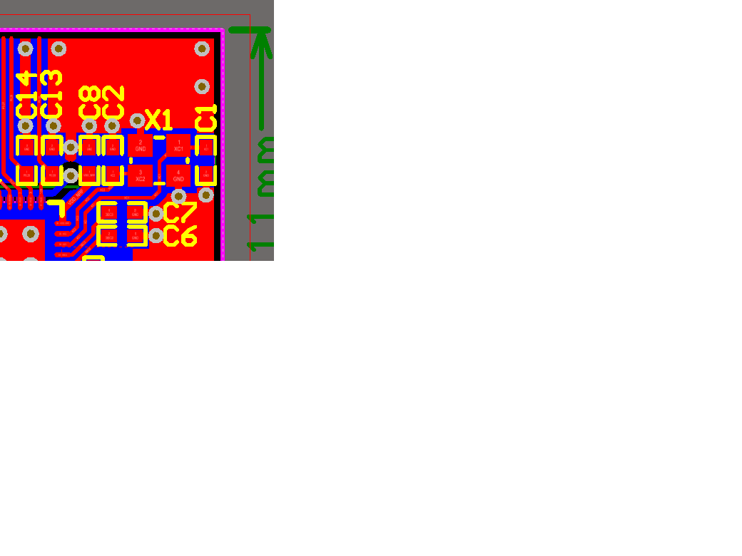
HI, I saw in a recommended layout for NRF52, that the traces goes as follow:
- the side that closed to NRF passes through load capacitor and then goes to the connected pin of Crystal.
- the side that is palced more far away, the trace goes first to the connected pin and then to the capacitor.
 Is there a purpose in this kind of layout?
From my previous designs i know that it is recommended first to go through the crystal pin and then to the load capacitor and here we have one pin this way and the other opposite.
Is there a purpose in this kind of layout?
From my previous designs i know that it is recommended first to go through the crystal pin and then to the load capacitor and here we have one pin this way and the other opposite.
thank you Yulya
