
Hiya,
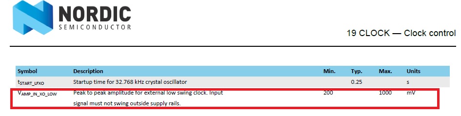
Regarding voltage amplitude peak to peak for external high-swing clock HFXO 32MHz, what's supply rails?I don't find out this specification defined in datasheet PS_V1.2.
Thanks Kenji
Hiya,
Regarding voltage amplitude peak to peak for external high-swing clock HFXO 32MHz, what's supply rails?I don't find out this specification defined in datasheet PS_V1.2.
Thanks Kenji

