Hi
I try to communicate with others TWi devices using the twi_hw_master driver.
When i initiate a communication with twi_master_transfer , i don't receive any ack from the target device (timeout in twi_master_write function ). So i looking for a problem on my twi bus
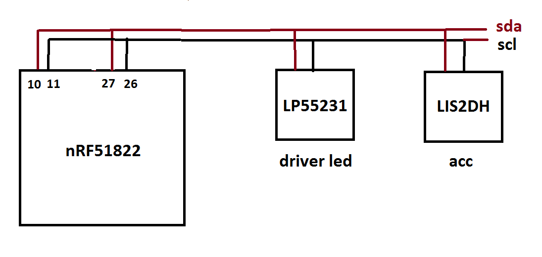
Attached my hardware implementation. You can see a particularity on my shematic : Sdl and Sda are both connected on two pins on the nrf. It's due to a place constraint. Internal pull-up are used. So i'm using only 2 pins but i'm afraid the 2 others pins interferes on the bus.
I've try this but is not changing anything :
nrf_gpio_cfg_input(26,NRF_GPIO_PIN_NOPULL );
nrf_gpio_cfg_input(27,NRF_GPIO_PIN_NOPULL );
My first question is how to be sure the two unused connected pins doesn't interferes with my twi bus ?
Secondly , i'm convinced pull-up are by default connected on tw_hw_master.c but can you confirm this ?
Tw_hw_master.c init function :
bool twi_master_init(void)
{
    /* To secure correct signal levels on the pins used by the TWI
       master when the system is in OFF mode, and when the TWI master is
       disabled, these pins must be configured in the GPIO peripheral.
    */
    NRF_GPIO->PIN_CNF[TWI_MASTER_CONFIG_CLOCK_PIN_NUMBER] =     \
        (GPIO_PIN_CNF_SENSE_Disabled << GPIO_PIN_CNF_SENSE_Pos) \
      | (GPIO_PIN_CNF_DRIVE_S0D1     << GPIO_PIN_CNF_DRIVE_Pos) \
      | (GPIO_PIN_CNF_PULL_Pullup    << GPIO_PIN_CNF_PULL_Pos)  \
      | (GPIO_PIN_CNF_INPUT_Connect  << GPIO_PIN_CNF_INPUT_Pos) \
      | (GPIO_PIN_CNF_DIR_Input      << GPIO_PIN_CNF_DIR_Pos);

    NRF_GPIO->PIN_CNF[TWI_MASTER_CONFIG_DATA_PIN_NUMBER] =      \
        (GPIO_PIN_CNF_SENSE_Disabled << GPIO_PIN_CNF_SENSE_Pos) \
      | (GPIO_PIN_CNF_DRIVE_S0D1     << GPIO_PIN_CNF_DRIVE_Pos) \
      | (GPIO_PIN_CNF_PULL_Pullup    << GPIO_PIN_CNF_PULL_Pos)  \
      | (GPIO_PIN_CNF_INPUT_Connect  << GPIO_PIN_CNF_INPUT_Pos) \
      | (GPIO_PIN_CNF_DIR_Input      << GPIO_PIN_CNF_DIR_Pos);

    NRF_TWI1->EVENTS_RXDREADY = 0;
    NRF_TWI1->EVENTS_TXDSENT  = 0;
    NRF_TWI1->PSELSCL         = TWI_MASTER_CONFIG_CLOCK_PIN_NUMBER;
    NRF_TWI1->PSELSDA         = TWI_MASTER_CONFIG_DATA_PIN_NUMBER;
    NRF_TWI1->FREQUENCY       = TWI_FREQUENCY_FREQUENCY_K100 << TWI_FREQUENCY_FREQUENCY_Pos;
    NRF_PPI->CH[0].EEP        = (uint32_t)&NRF_TWI1->EVENTS_BB;
    NRF_PPI->CH[0].TEP        = (uint32_t)&NRF_TWI1->TASKS_SUSPEND;
    NRF_PPI->CHENCLR          = PPI_CHENCLR_CH0_Msk;
    NRF_TWI1->ENABLE          = TWI_ENABLE_ENABLE_Enabled << TWI_ENABLE_ENABLE_Pos;

    return twi_master_clear_bus();
}
Thanks