This post is older than 2 years and might not be relevant anymore
More Info: Consider searching for newer posts

MIFA Antenna for nrf52832

I am designing the BLE solution using nrf52832. The board will be two layer board with solid ground plane in the bottom layer and signal and ground pour in the top layer. I am planning to use MIFA antenna for my PCB. I have few questions regarding MIFA as this is the first time I am designing an Antenna.

  1. What is Antenna Feed line?. Is it the PCB trace from ANT pin of SoC to Matching network? How to calculate it's width? Should it be 50 ohm transmission line and do I need to calculate it's width using coplanar transmission line equation (because i will be having ground pour on both layers)?

  2. Do I need to tune my MIFA antenna by adjusting it's length (so that it can resonance at 2.4 GHz)? I am looking for some specific equation which includes PCB thickness, relative dielectric constant and other important parameters and give me length of MIFA antenna.

  3. Do I need to place matching network passive components near to antenna? From ANT pin of SoC, there should be transmission line (called Antenna Feed) of 50 ohm (because impedance of ANT pin is 50 ohm). Then, there will be a matching network which will match the impedance of Antenna to 50 ohm. And just after the matching network, there should be antenna. Does my understanding is correct?

  4. I can't find any antenna recommended by nordic. Does nordic provide any antenna for their SoC?

  5. I have referred the MIFA antenna from this document.

image description

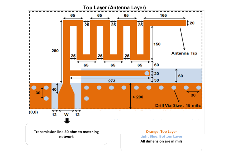
I hope the antenna showed above (taken from document mentioned above) will give good performance for BLE. Please have a look at the antenna and guide me if i am doing something wrong.

  • I believe that's called a 'MIFA' antenna, MILF is something entirely different and not a very nice term to use. So perhaps you might like to go edit your original question and use the correct, and less offensive, term.

  • Hello abhiarora

    1. The antenna feed line is the PCB trace that carries the RF signal to the antenna. For the nRF52832 the signal comes from pin 30 of the QFN package, or D1 from the WLCSP package. You need a matching network to match the chip to 50 Ohm, it should be placed as close to the chip as possible. See section 53 of the nRF52832 product specification. You then need a line, carefully matched to 50 Ohm, which leads to the antenna's matching network. The antenna and its network must match the antenna to 50 Ohm. It is important there is an unbroken ground plane on the bottom layer underneath all components that make up the matching networks, and all traces that connect them. Do note that there should be no ground plane underneath the antenna itself.

    If you have a ground plane on the same plane as the trace then you will need to calculate it as a coplanar transmission line, remember to include the bottom ground plane in your calculations if present.

    For more guidelines on PCB design for the nRF52 series, see this tutorial

    1. The MIFA is a bit more complicated to work with compared to a standard monopole antenna, but cutting the antenna length is still viable here. Section 7.3 of the document you linked to comments on this, so you should design the antenna a bit longer than necessary, so that you have something to work with. Unfortunately we do not have any guides on designing MIFA's available.

    2. See my first answer. Your understanding is correct.

    You will need to either simulate the antenna, or build a prototype that you can measure. Antennas are very sensitive to the physical layout, as well as objects in their vicinity. Commenting on the design in the figure is therefore not very fruitful. What I can say is that according to the link you posted it is designed for 2.4 GHz, with FR4 substrate with 1.6mm thickness, which is quite common. If you go for that design you should follow it closely.

    Our development kits come with a monopole antenna. You can find the nRF52 DK hardware files which contains layout files here, a whitepaper on monopole design can be found here. The Nordic Thingy:52 comes with a ceramic chip antenna from Johanson. You can find more information on the thingy here, and its hardware files here.

    Best regards

    Jørn Frøysa

  • Do you know any simulation or MIFA designing tools? Yes, our PCB fabrication house has 1.55mm FR4 substrate.

    Do I need two matching networks? What if I match the ANT Pin to impedance of antenna feed and antenna feed has same impedance as of antenna? Then, will one matching network work?

  • Unfortunately I am not aware of any design tools specifically for MIFA's. There are several EM solvers out there which can be used for antenna design such as CST microwave studio or Ansys HFSS. If you are able to design the antenna itself with a 50 Ohm input impedance then you only need a matching network for the nRF52 chip. For a prototype you would typically design it so you can add matching, or tune the antenna as it is highly likely the input impedance will deviate from the one you simulated, due to layout, product casing etc.

Related