Hi,
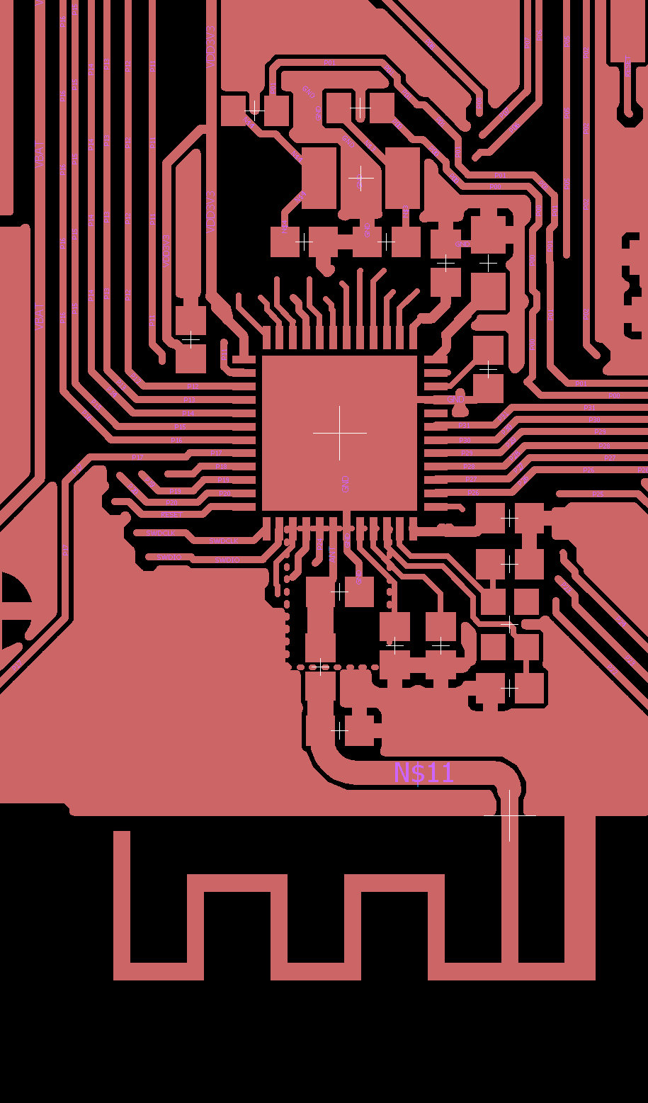
I have designed a custom PCB using NRF52832 IC.I have followed Sparkfun NRF52832 breakout board for placement of NRF52832 IC core part(including antenna) which is similar to the recommended reference design in the datasheet. SparkFun board link: learn.sparkfun.com/.../nrf52832-breakout-board-hookup-guide
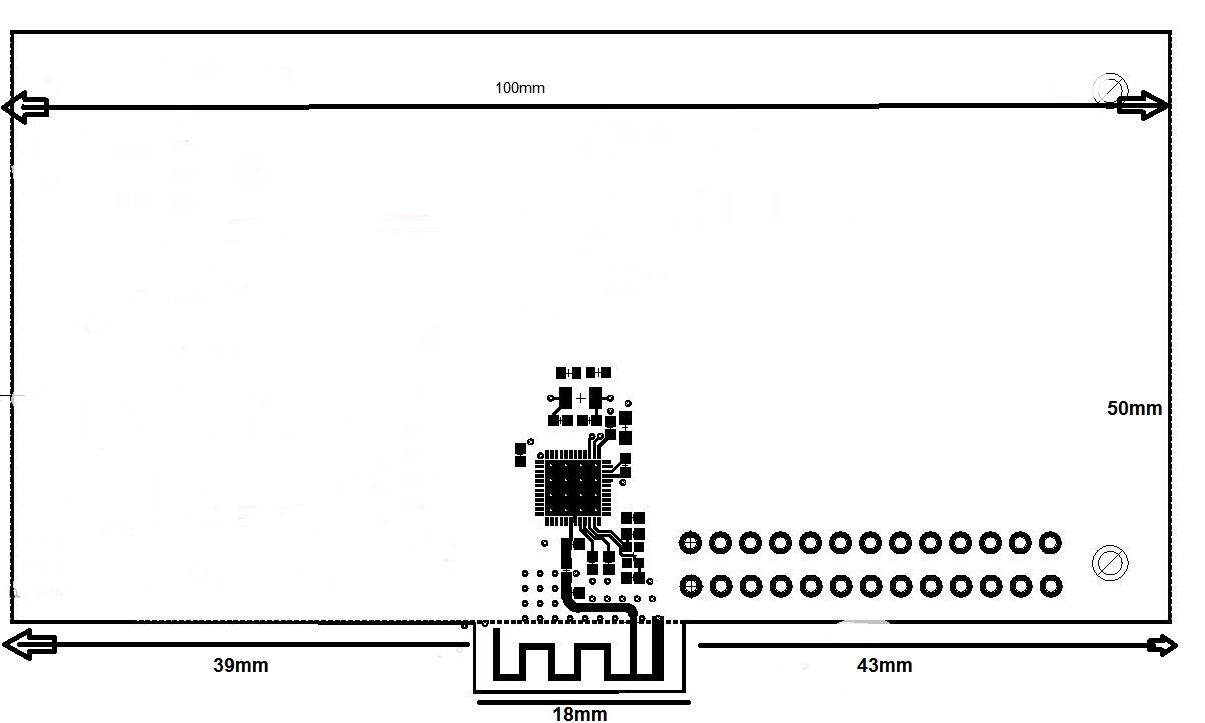
My board dimensions: 100x50 mm.
Is this design OK? Need improvements/suggestions for my design.
 .
.
Layout: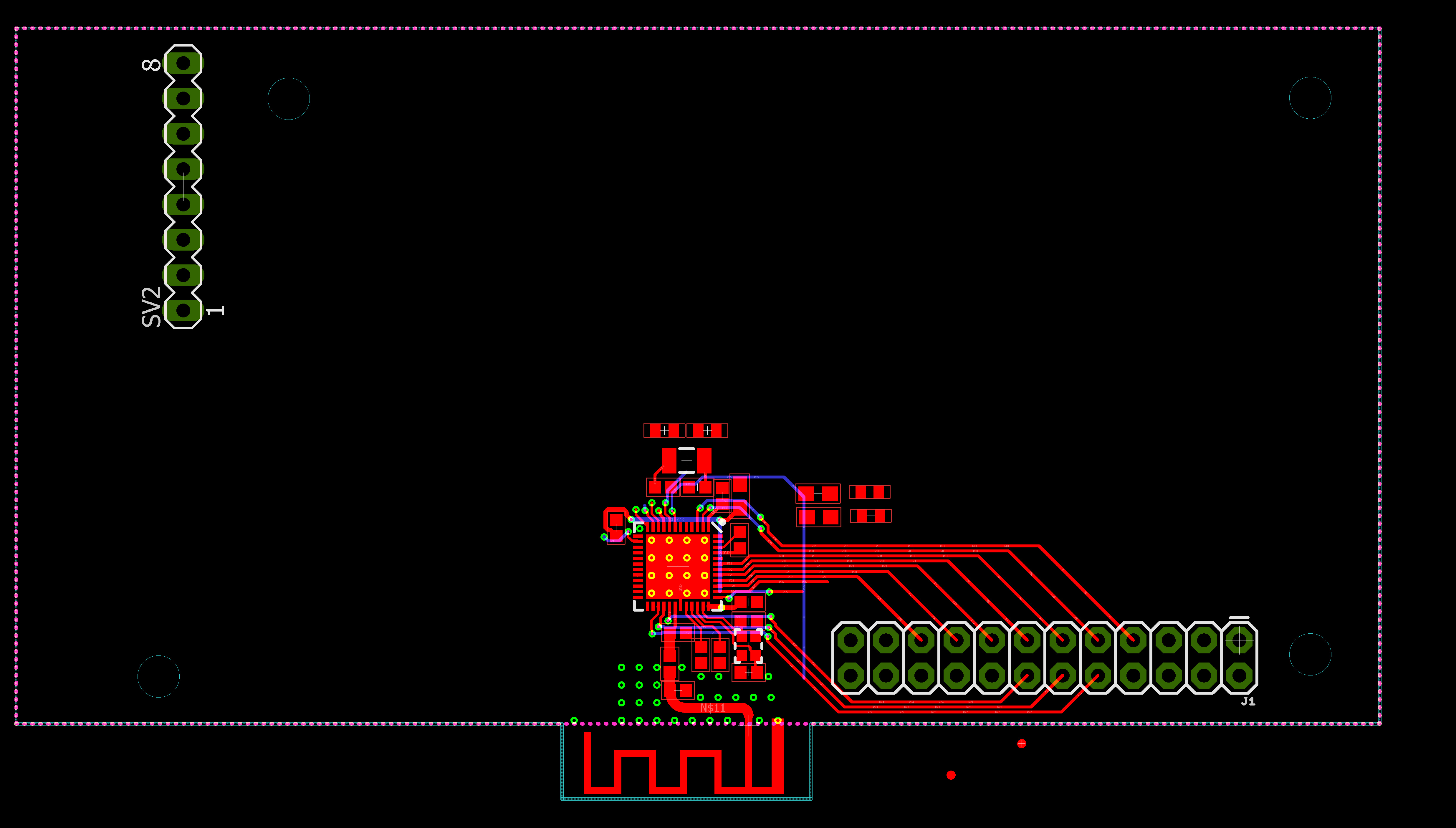
Ground planes: 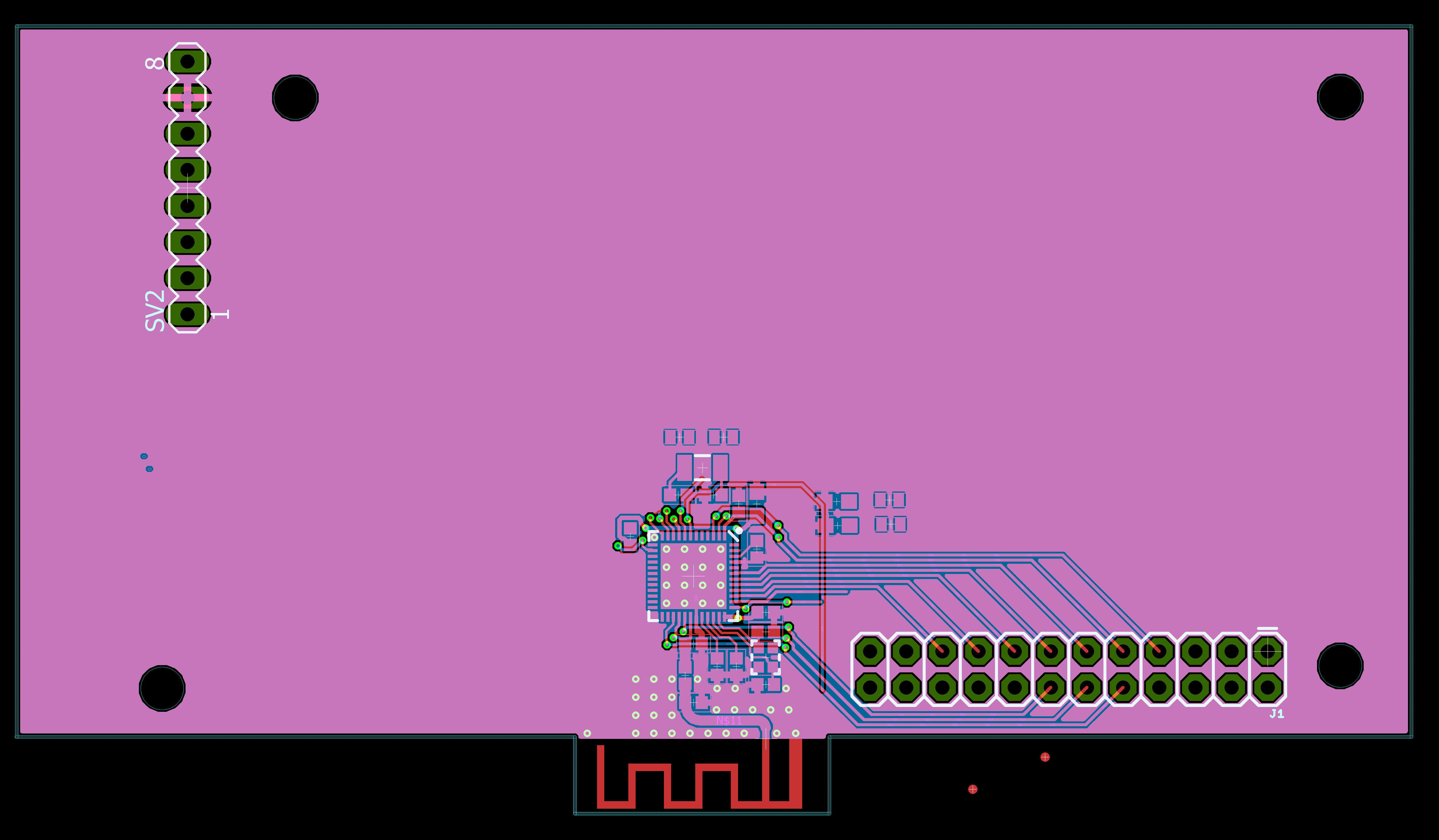
Layout after adding polygon cut-outs around matching circuit elements: