This post is older than 2 years and might not be relevant anymore
More Info: Consider searching for newer posts

PCB stackup for NRF52832 two layered board

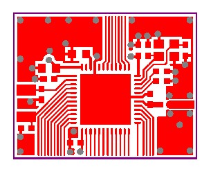
Hello, I am designing a custom 2layered PCB board with NRF52832 IC. I have followed the reference design given in IC's datasheet as shown in the figure. Please provide the PCB stack up details for 2 layered board.

image description

Parents
  • All the Nordic 2 layer designs I am aware of are based on 0.062 inch (~1.6mm) FR4 boards. The reason for this is it has become bit of an industry standard over the years and at this point most of the through hole connectors are designed for it and also it is easy for board vendors to get inexpensive 0.062 material. Plus 0.062 has a reasonable rigidity for products.

    So that being said you are sourcing an 0.062 inch FR4 board.

    However, all FR4 boards are not the same and vary by vendor. You should get an idea of the final Er for your board from your vendor and model the waveguides using your assumptions to make sure it will work. Er for FR4 ranges from about 4.2 to 4.6 at 2.4GHz. Optionally you could spec the coplanar output as 50ohm on your design drawings and your vendor will be able to ensure it is 50ohms. This is normally an extra service at some cost.

    What really worries me about your design is the sheer dearth of vias, especially under the nRF where I do not see any. You should take another look at the reference design and get the ground vias correct and if you wish to have the design reviewed, please repost with the ground layer as well.

  • Hello Thank you for the info. I didn't get the term waveguide". What do you mean by a waveguide? Is it pcb antenna?

Reply Children
No Data
Related