This post is older than 2 years and might not be relevant anymore
More Info: Consider searching for newer posts

Error 133 (0x85): GATT ERROR

Hello everyone,

I know this issue is quite recurrent but I've gone crazy reading so many different issues with android version, Connection intervals, etc. Would like to know if someone can help me looking for an answer that fits the description of my problem or just forward me into a direction to solve the issue.

So, I've tried my firmware on the nRF SDK and everything works perfectly (Samsung note 2 connects fine and also a Xiaomi phone) but whenever I try to connect to my custom board, the phones cannot connect to it and I get this nRF Connect log:

    nRF Connect, 2017-11-27
Malapascua (D9:1C:BF:F2:0E:03)
V	16:20:44.774	Connecting to D9:1C:BF:F2:0E:03...
D	16:20:44.774	gatt = device.connectGatt(autoConnect = false, TRANSPORT_LE) (hidden)
D	16:21:05.631	[Callback] Connection state changed with status: 133 and new state: DISCONNECTED (0)
E	16:21:05.631	Error 133 (0x85): GATT ERROR
I	16:21:05.631	Disconnected

The only noticeable difference is the RSSI: nRF SDK moves between -30 up to -43 dBm while my custom board is between -70 up to -80 (really bad connectivity).

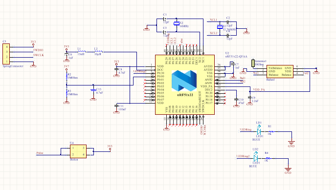
Here is my schematic:

image description

And here is also my layout (units in mm):

  • Purple is stiffener plane
  • Blue is Bottom Layer
  • Red is Top Layer

image description

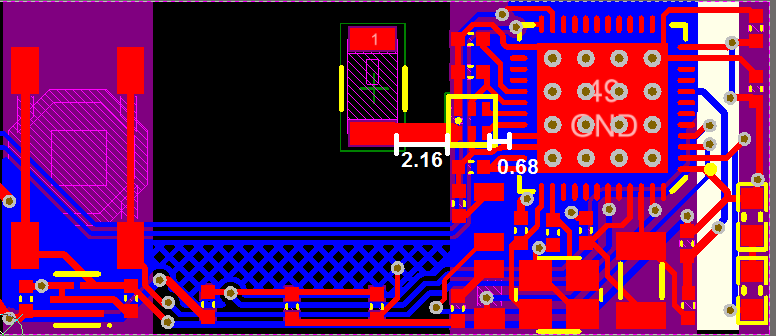
The antenna track is 0.762 mm width with 1 oz thickness.

Thank you,

Pablo G

Parents
  • Hello PabloGC

    There are a few things that should be corrected on your board. From what I can see you do not have a ground plane on your top layer, please correct me if this is incorrect, which is highly recommended (and for the antenna necessary) to have. A ground plane will give a more solid ground for the RF signals to couple to, and functions as the second part of the antenna. By omitting the ground plane you diverge from the reference layout stated in the nRF51 product specification, and the antenna specification.

    Antennas are highly sensitive to the layout surrounding them, as well as the over-all environment they work in. Small changes in layout can cause considerable change in the antenna characteristics and impedance, and the reference design should be followed as closely as possible. See this link for more information from Johanson Technology on layout considerations for their antennas. You will find that the ground plane, the feed-line, the antenna placement relative to the ground plane as well as the antenna orientation are all important to the antenna performance.

    You also have omitted the antenna matching network. Due to the antennas dependence on its surroundings, it is unlikely to have an impedance of 50 Ohm by itself, and therefore needs a matching network as stated in the product specification.

    You have routed a couple of signal lines underneath your RF section, in parallel with the edge of your stiffener on the right hand side of the antenna. The ground plane underneath any RF component should be unbroken and as large as possible. Any openings and traces located underneath the RF section is highly likely to cause impedance mismatch, which again causes loss as well as unwanted emissions. The exception to this is the antenna which should have a keep-out region surrounding it as explained in the product specification.

    I would recommend you redo the layout, and have an additional ground plane on your top layer. This ground plane should be well connected to the bottom layer ground plane through vias, especially along the edge towards the antenna. You should read the specifications carefully, and follow the reference layouts as stated in the product specification for both the nRF51 and the antenna. More PCB guidelines for the nRF51 series can be found here

    Best regards

    Jørn Frøysa

Reply
  • Hello PabloGC

    There are a few things that should be corrected on your board. From what I can see you do not have a ground plane on your top layer, please correct me if this is incorrect, which is highly recommended (and for the antenna necessary) to have. A ground plane will give a more solid ground for the RF signals to couple to, and functions as the second part of the antenna. By omitting the ground plane you diverge from the reference layout stated in the nRF51 product specification, and the antenna specification.

    Antennas are highly sensitive to the layout surrounding them, as well as the over-all environment they work in. Small changes in layout can cause considerable change in the antenna characteristics and impedance, and the reference design should be followed as closely as possible. See this link for more information from Johanson Technology on layout considerations for their antennas. You will find that the ground plane, the feed-line, the antenna placement relative to the ground plane as well as the antenna orientation are all important to the antenna performance.

    You also have omitted the antenna matching network. Due to the antennas dependence on its surroundings, it is unlikely to have an impedance of 50 Ohm by itself, and therefore needs a matching network as stated in the product specification.

    You have routed a couple of signal lines underneath your RF section, in parallel with the edge of your stiffener on the right hand side of the antenna. The ground plane underneath any RF component should be unbroken and as large as possible. Any openings and traces located underneath the RF section is highly likely to cause impedance mismatch, which again causes loss as well as unwanted emissions. The exception to this is the antenna which should have a keep-out region surrounding it as explained in the product specification.

    I would recommend you redo the layout, and have an additional ground plane on your top layer. This ground plane should be well connected to the bottom layer ground plane through vias, especially along the edge towards the antenna. You should read the specifications carefully, and follow the reference layouts as stated in the product specification for both the nRF51 and the antenna. More PCB guidelines for the nRF51 series can be found here

    Best regards

    Jørn Frøysa

Children
  • Thank you very much Jorn, I will take more care when redoing the layout. I just wanted to make sure the error 133 was happening because of the bad connectivity and not something I was missing in the schematic. As I said, the program I'm uploading works absolutely fine with the nRF SDK so it should also work with my custom board, right? (I just want to discard any firmware incompatibilities)

  • The fact that it is working perfectly on your devkit does indicate that your firmware is OK, especially if the chip on your devkit and custom board are the same revision versions. You registered an RSSI of -70 to -80 dBm on your custom board. Considering the nRF51 has a sensitivity of -93 that only gives you a headroom of 23 to 13 dB. In an indoor or urban environment that isn't all that much.

    You could try to use a sniffer and see what exactly is exchanged between the two devics before the disconnect. This would give you a further indication as to whether the disconnect is a firmware error or not.

  • Do you know any phone app that I can use as a sniffer? I already tryied Wireshark in my computer but I was having so many problems with the set up that I drop it...

  • Unfortunately I don't know of a mobile app. The sniffer software is a bit old, so it can be a bit troublesome to get going. It requires version 1.10 of wireshark, later versions won't work. The sniffer devkit must be a nRF51 (f.ex. the pca10028) and the on board J-link debugger firmware should be downgraded to version 5.1, you can find a link to version 5.10n in this blogpost. After you've installed the j-link software you can open the J-link configurator from the correct folder in the start menu (for windows) and replace the firmware of the kit.

Related