This post is older than 2 years and might not be relevant anymore
More Info: Consider searching for newer posts

51822 PWM unstable

Hi guys,

I use the 51822's PWM recently, PWM is made by GPIOTE+PPI+TIMER, and the PWM source code as below(I use TIMER1, GPIOTE[0], PPI_CH[0], PPI_CH[1], period and duty means ticks with 16MHz):

void startPwm1(uint16_t period, uint16_t duty)
{
	NRF_TIMER1->INTENCLR = TIMER_INTENSET_COMPARE0_Enabled << TIMER_INTENSET_COMPARE0_Pos; 
	NVIC_DisableIRQ(TIMER1_IRQn);
	
	NRF_GPIOTE->CONFIG[0] = GPIOTE_CONFIG_MODE_Task << GPIOTE_CONFIG_MODE_Pos |
							GPIOTE_CONFIG_POLARITY_Toggle << GPIOTE_CONFIG_POLARITY_Pos |
							WAVE_PWM << GPIOTE_CONFIG_PSEL_Pos | 
							GPIOTE_CONFIG_OUTINIT_Low << GPIOTE_CONFIG_OUTINIT_Pos;
	
	NRF_PPI->CH[0].EEP = (uint32_t) &NRF_TIMER1->EVENTS_COMPARE[0];
	NRF_PPI->CH[0].TEP = (uint32_t) &NRF_GPIOTE->TASKS_OUT[0];
	
	NRF_PPI->CH[1].EEP = (uint32_t) &NRF_TIMER1->EVENTS_COMPARE[1];
	NRF_PPI->CH[1].TEP = (uint32_t) &NRF_GPIOTE->TASKS_OUT[0];
	NRF_PPI->CHENSET = (PPI_CHENSET_CH0_Enabled << PPI_CHENSET_CH0_Pos) | (PPI_CHEN_CH1_Enabled<< PPI_CHEN_CH1_Pos);
	
	NRF_TIMER1->TASKS_STOP = 1;
	NRF_TIMER1->TASKS_CLEAR = 1;
	
//	NRF_TIMER1->PRESCALER = 0;
	NRF_TIMER1->CC[0] = period;  	
	NRF_TIMER1->CC[1] = period - duty;	
	NRF_TIMER1->SHORTS = TIMER_SHORTS_COMPARE0_CLEAR_Enabled << TIMER_SHORTS_COMPARE0_CLEAR_Pos;
	NRF_TIMER1->INTENCLR = TIMER_INTENSET_COMPARE0_Enabled << TIMER_INTENSET_COMPARE0_Pos; 
	NRF_TIMER1->TASKS_START = 1;
}

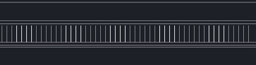
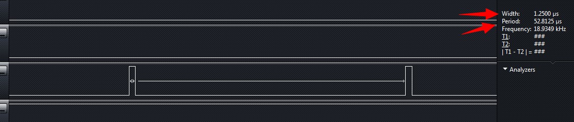
When I download the program to the development board, PWM works well(period is 842 ticks, duty is 20 ticks), As shown below:

image description image description

Then power off the development board, and connected other 3.3V power supply to any 51822's GPIO port, then disconnected, power the development board, Now the PWM does not work well, as show below: image description

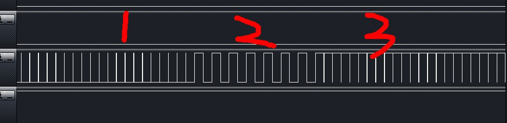
1 pwm works well, 3 looks like Inverted. It seems like GPIOTE's response is not in time.

So have you encountered this situation?

  • There are different levels of power manage. The SD docs discuss these. You can keep the ppi/gpiote running whilst do a power manage.

    Still need clarity on HFCLK. Earlier you responded by discussing the LFCLK (ie, RTC). The pclock is generated from the 16MHz clock. You need to make sure it is running on the external crystal and not the internal 16MHz RC clock.

    If you feel like posting a pdf of your schematic that would be good too. To make sure there are no mistakes.

  • Per my question above you should read over page 32 of the nrf51822 spec: 4.2 Timer/counters (TIMER) The timer/counter runs on the high-frequency clock source (HFCLK) and includes a 4 bit (1/2X) prescaler that can divide the HFCLK. The TIMER will start requesting the 1 MHz mode of the HFCLK for values of the prescaler that gives fTIMER less or equal to 1 MHz. If the timer module is the only one requesting the HFCLK, the system will automatically switch to using the 1 MHz mode resulting in a decrease in the current consumption. See the parameters I1v2XO16,1M, I1v2XO32,1M, I1v2RC16,1M in Table 32 on page 47 and ITIMER0/1/2,1M in Table 52 on page 61. The task/event and interrupt features make it possible to use the PPI system for timing and counting tasks between any system peripheral including any GPIO of the device. The PPI system also enables the TIMER task/event features to generate periodic output and PWM signals to any GPIO. The number of input/outputs used at the same time is limited by the number of GPIOTE channels.

  • Hi, here is the sch pdf, link text
    I found that there is an external crystal.

    I did not configure HFCLK in the application code, Is there any problem?

    The program is working fine on the nrf51 DK board, but not working well on my own board.

  • You should always configure the external crystal if you intend to use it. Some peripheral blocks/drivers will automatically configure it for you but many will run on the HF internal RC which would be a bad idea for pwm. According to the spec the timers run off the whatever the current HF CLK is.

    With regard to your board, there will ALWAYS be an external 16MHz crystal. This is because it is required for bluetooth communications. However you still have to configure it otherwise the chip will default to 16MHz RC clk.

    Your module has very few direct connections to gpio. In this manner it is COMPLETELY different from the DK. You need to specify which pins you are using since what I see in the schematic is some very aggressive filtering of the gpio output for things labeled "pwm" and the other stuff is designed as "open collector". "open collector" is a rather odd and very outdated choice since BJT's are pretty bad at switched signals when compared to fet's.

  • The PWM pin is P0.05 and P0.11.

    Thanks for your suggestion, I will remove the PWM pin's capacitance and test it.

Related