This post is older than 2 years and might not be relevant anymore
More Info: Consider searching for newer posts

Error frames receiving on sniffer from nRF52832 custom board

image description

Hello All,

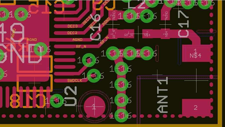
Please check above image, showing antenna layout of my custom board. I am receiving error frames at ~40ft distance on sniffer. Please check whether antenna layout is ok or not. Please let me know if more info required.

Antenna Part: 2450AT18A100, Make: Johanson Technology.

Edits for comment: Schematic: nrf_antennaFor review .pdf

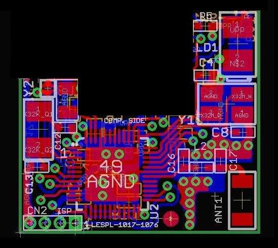
Layout Image showing ground plane and surrounding components: image description

Regards,

Sharad.

Parents
  • Hello Sharad

    If you take a look at the nRF52832 product specification page 551, section 53.7 you will find the PCB layout guidelines. Your trace leading out from the ANT pin to the matching network seems a bit long. This will cause impedance transformation, which will lead to a mismatch with 50 Ohm. The trace should be kept as short as possible.

    From what I can see on the layout picture there also seem to be a bit of ground plane missing underneath the trace due to the SWDIO via hole. Traces carrying RF signals should always have a unbroken ground plane underneath. Failing to have so will alter the characteristic impedance of the trace and can cause unwanted emissions. I recommend you follow the PCB guidelines as closely as possible. Also see this tutorial for more PCB design guidelines.

    You have not designed the antenna matching network as stated in the antenna product specification. Have you measured the antennas input impedance as seen from the output of the nRF matching network with a VNA to ensure it presents itself as a 50 Ohm load? Mismatch between the nRF matching network and the antenna will be a source of loss and cause attenuation in your signal.

    The layout surrounding the antenna is not according to the antenna product specification. The antenna is designed to be placed 90 degrees on the feedpoint, with a ground plane surrounding the feeding point. Do note that changes like this can affect the antenna impedance and thus the antennas radiation characteristics. There is also a ground plane on the bottom layer which is very close to the antenna, please see the recommended keep-out region shown in the antenna product specification.

    If you have not done so I would recommend measuring the antenna with a VNA to ensure it has been properly matched. Do note that when doing this the antenna should be located in an environment which matches the environment it will ultimately be used in as closely as possible. Antennas are very sensitive to their surroundings, and any objects, ground planes, casings etc. located in their proximity can alter their impedance and behavior.

    Best regards

    Jørn Frøysa

Reply
  • Hello Sharad

    If you take a look at the nRF52832 product specification page 551, section 53.7 you will find the PCB layout guidelines. Your trace leading out from the ANT pin to the matching network seems a bit long. This will cause impedance transformation, which will lead to a mismatch with 50 Ohm. The trace should be kept as short as possible.

    From what I can see on the layout picture there also seem to be a bit of ground plane missing underneath the trace due to the SWDIO via hole. Traces carrying RF signals should always have a unbroken ground plane underneath. Failing to have so will alter the characteristic impedance of the trace and can cause unwanted emissions. I recommend you follow the PCB guidelines as closely as possible. Also see this tutorial for more PCB design guidelines.

    You have not designed the antenna matching network as stated in the antenna product specification. Have you measured the antennas input impedance as seen from the output of the nRF matching network with a VNA to ensure it presents itself as a 50 Ohm load? Mismatch between the nRF matching network and the antenna will be a source of loss and cause attenuation in your signal.

    The layout surrounding the antenna is not according to the antenna product specification. The antenna is designed to be placed 90 degrees on the feedpoint, with a ground plane surrounding the feeding point. Do note that changes like this can affect the antenna impedance and thus the antennas radiation characteristics. There is also a ground plane on the bottom layer which is very close to the antenna, please see the recommended keep-out region shown in the antenna product specification.

    If you have not done so I would recommend measuring the antenna with a VNA to ensure it has been properly matched. Do note that when doing this the antenna should be located in an environment which matches the environment it will ultimately be used in as closely as possible. Antennas are very sensitive to their surroundings, and any objects, ground planes, casings etc. located in their proximity can alter their impedance and behavior.

    Best regards

    Jørn Frøysa

Children
No Data
Related