This post is older than 2 years and might not be relevant anymore
More Info: Consider searching for newer posts

nRF52840 Chip Impedance (BT and NFC)

Hi,

to what impedance shall the BT antenna be matched?

Copying from the datasheet: A matching network is needed between the RF pin ANT and the antenna, to match the antenna impedance (normally 50 ohm) to the optimum RF load impedance for the chip. For optimum performance, the impedance for the matching network should be set as described in the recommended AQFN73 package reference circuitry from Circuit configuration no. 1 on page 688. image description
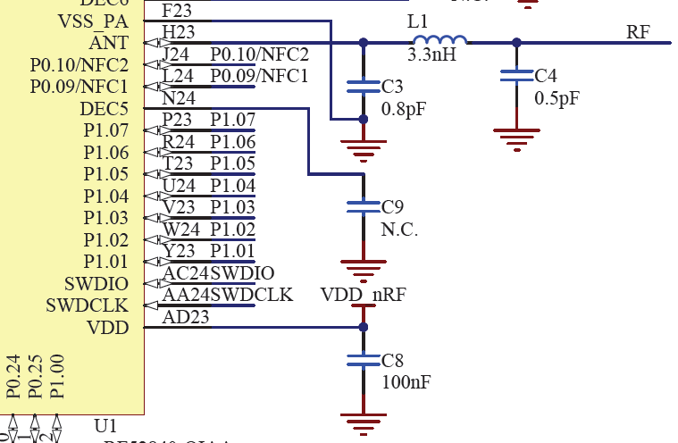
The Pi network is fine. The values given would work for a given antenna, a given layout, and a given placement/casing. So what impedance the chip "desires to see"? Is it significantly dependent on the BT mode of operation? Any table on that?

Same question for the differential NFC1/2 impedance.

Thanks,

Zeid

  • By using the reference design above the chip is matched to a 50 Ohm reference point.

    Then you need to match the antenna to the 50 Ohm reference point.

    You can read more about it here.

    Is it significantly dependent on the BT mode of operation? Any table on that?

    I'm not sure what this means. Could you explain a bit more?

    I'm not really an expert on NFC, but maybe this answers your question?

    There is also a reference design with NFC here.

  • Thanks Petter for the info. Copying from the link in the tutorial: The pcb layout (pad size, lines etc) is a part of the matching, make sure that your design is an exact copy of the reference design. I do agree that the layout is part of the matching. However in order for the copying rule to work well, the two designs should use the exact same material and layer thickness. I am not sure that this is feasible neither can I enforce that in my design. Therefore some indication on the chips' impedance around 2.44 GHz would be helpful.

    Concerning the impedance dependency: Usually for a set of parameters (given output power, an operating frequency, a supply voltage level...) there's one optimal impedance. The closer these optimal impedances to each other are over parameter changes, the better. I assume for using different modes (1 Mbps vs 125 kbps), the desired impedance is the same?

  • Hello Zeid

    All reference designs are made for FR4 with a total substrate thickness of 1.6mm. As long as you use that, keep component sizes small, and trace lengths short, the impact of a deviation in dielectric constant should be negligible.

    Unfortunately we do not have any measurements for the impedance at different modes of the nRF52840 yet, see the answer on this post.

    If you deviate from either board type used or layout, you can measure the input of the RF pin, from outside of the match, while TX or RX is active with a VNA to ensure it presents itself as 50 Ohm. Do note however this will typically not tell you how efficiently the network filters harmonics, and you may want to do a measurement with a spectrum analyzer as well.

    BR Jørn Frøysa

Related